

Via Pushes Small Form Factor Motherboard Design Deep Dive
Via pushes small form factor motherboard design is becoming increasingly popular for its ability to pack more components into a smaller space. This design approach involves strategically placing vias to optimize component placement, thermal management, and power delivery. Understanding the nuances of via placement, from Mini-ITX to Pico-ITX boards, is key to harnessing the full potential of these compact systems.
This in-depth exploration examines the various facets of via-centric small form factor motherboard design, from the foundational principles to the practical considerations in manufacturing and assembly. We’ll delve into the specific challenges and advantages, along with practical solutions and case studies.
Introduction to Small Form Factor Motherboards: Via Pushes Small Form Factor Motherboard
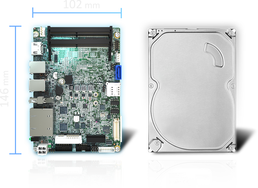
Small form factor (SFF) motherboards are a class of computer motherboards designed with reduced dimensions compared to standard ATX boards. This compact design prioritizes space-saving, often leading to more portable and aesthetically pleasing computer builds. Their popularity stems from the ability to create smaller, yet powerful, systems suitable for various applications, from home theater PCs to compact gaming rigs.These motherboards are carefully engineered to balance size constraints with functionality.
Key design considerations include component placement, power delivery, and thermal management, all while ensuring compatibility with standard components. This necessitates innovative approaches to board layout and component selection. Understanding the different types and their specific characteristics is crucial for selecting the right motherboard for your needs.
Types of Small Form Factor Motherboards
Various small form factor motherboard types cater to different needs and builds. The most common types include Mini-ITX, Pico-ITX, and others. Each type has distinct size constraints, feature sets, and price points.
Mini-ITX vs. Pico-ITX
| Feature | Mini-ITX | Pico-ITX |
|---|---|---|
| Size | 170mm x 170mm | 100mm x 72mm |
| Features | Typically supports a wider range of CPUs, including dual-core processors. Supports a broader range of expansion slots, including PCI-e slots. Often includes more storage options like SATA ports. | Limited to single-core or lower-powered CPUs. Expansion slots are extremely limited, often restricted to only one or two slots. Generally, has fewer storage options. |
| Price | Generally more affordable than Pico-ITX motherboards, offering a balance between size and features. | Primarily targeted for the budget-conscious user, but generally more expensive than a comparable ATX motherboard. |
| Applications | Ideal for home theater PCs, HTPC builds, and compact desktops needing a balance of features and size. | Excellent for extremely compact systems, such as ultra-small PCs, embedded systems, and where space is absolutely paramount. |
These different types of SFF motherboards allow for customization in building a system. The choice depends on the user’s needs and priorities for features, size, and cost.
Via Technology in Motherboards
Via technology plays a crucial role in the design of modern circuit boards, particularly in small form factor motherboards. It allows for the efficient routing of signals and power delivery while minimizing the overall size and complexity of the board. This is especially important in the ever-shrinking world of small form factor designs, where space is at a premium.
The use of via pushes is a key element in achieving these goals.Via technology essentially creates electrical pathways between different layers of a printed circuit board (PCB). These pathways, or vias, are crucial for connecting components and routing signals throughout the board. Via pushes, a specific implementation of via technology, are designed to reduce the overall size and improve the performance of the PCB, particularly in small form factor designs.
Via Implementation in Small Form Factor Designs
Via pushes are implemented in small form factor designs to maximize space utilization and minimize signal interference. This technique involves strategically placing vias in a way that allows for a more compact layout. The design process involves careful consideration of component placement and signal routing to ensure optimal performance while maintaining a small footprint.
Benefits of Via Pushes in Small Form Factor Motherboards
Via pushes offer several significant advantages in small form factor motherboards:
- Reduced Board Size: Via pushes allow for more compact layouts, reducing the overall dimensions of the motherboard. This is critical in designs constrained by space limitations, such as laptop or mini-PC motherboards.
- Improved Signal Integrity: Strategically placed via pushes can help to minimize signal reflections and crosstalk, thereby improving the integrity and reliability of signal transmission. This is essential for maintaining high data transfer speeds in demanding applications.
- Enhanced Power Delivery: Via pushes can be used to improve the efficiency of power delivery by creating more direct paths for current flow. This is particularly crucial in power-hungry components, such as graphics processors, to minimize power losses and maintain stable voltage levels.
Impact on Performance and Efficiency
The impact of via pushes on performance and efficiency is multifaceted. Reduced board size contributes to a smaller thermal footprint, which can improve cooling and thermal management. Improved signal integrity directly translates to faster data transfer rates and reduced errors, essential for modern computing applications. Enhanced power delivery ensures stable operation of high-performance components, further contributing to overall system efficiency and reliability.
For instance, a mobile workstation motherboard designed with via pushes can achieve similar performance to a larger desktop motherboard while maintaining a compact size.
Diagram of Via Pushes
Imagine a cross-section of a PCB. Multiple layers are stacked together, representing different signal and power planes. Vias are depicted as small cylindrical holes that connect these layers. Via pushes are distinguished by their vertical height. In a via push, the via extends significantly further into a lower layer compared to a traditional via.
This extended reach allows for more efficient signal routing and power delivery, while maintaining a compact design. A schematic diagram of this would visually demonstrate the relative depth of the vias in relation to the layers of the PCB. This visual representation would clarify how via pushes optimize signal and power flow while maximizing space efficiency.
Component Placement and Density
Small form factor motherboards, like Mini-ITX and Pico-ITX, prioritize space efficiency, often squeezing more components into a smaller area than their full-size counterparts. This necessitates innovative design approaches for efficient component placement and heat management. The constrained space significantly impacts the selection and arrangement of components, especially with the integration of Via technology.The density of components on a motherboard directly correlates to its performance and features.
Optimizing this density requires careful consideration of component size, electrical pathways, and heat dissipation. Efficient placement of components and effective use of Via technology are key to achieving this.
Challenges of Component Placement
The reduced space on small form factor motherboards presents significant challenges for component placement. Limited space directly impacts the selection of components, forcing designers to choose smaller, more power-efficient parts. This constraint also complicates routing and signal integrity, as pathways must be meticulously planned to avoid signal interference. Moreover, the confined environment can hinder effective heat dissipation, potentially leading to overheating issues.
Impact of Via Pushes on Component Placement
Via technology, crucial for interconnecting components on small form factor motherboards, significantly influences component placement. Via pushes allow for routing signals through multiple layers, reducing the need for extensive traces on the surface. This reduced surface trace density allows for more space for other components, especially when combined with surface-mount components. However, vias introduce potential signal integrity challenges that must be carefully addressed during the design process.
Strategies for Optimizing Component Placement with Via Pushes
Efficient utilization of via pushes involves several strategies. Careful planning of signal paths, minimizing the length of traces, and optimizing via placement are critical. Furthermore, selecting components with compatible pinouts and optimizing the component arrangement to maximize spacing between components are essential steps. Using 3D-modeling tools and simulations is crucial to identify potential issues and refine the layout before physical production.
Comparison of Component Placement Strategies across Different Small Form Factor Motherboards
Mini-ITX motherboards, with their slightly larger footprint compared to Pico-ITX, generally offer more space for component placement, though the fundamental principles of minimizing trace length and maximizing component density still apply. The choice of components and their arrangement often differs significantly between these two categories, especially in the placement of components demanding high power or heat dissipation. Pico-ITX motherboards often rely on smaller components and more complex via strategies to achieve similar performance levels.
Component Density Table
| Motherboard Type | Component Count | Via Count |
|---|---|---|
| Mini-ITX | Approximately 150-250 | Approximately 500-1000 |
| Pico-ITX | Approximately 100-150 | Approximately 300-600 |
Note: The component counts and via counts in the table are approximate and can vary significantly depending on the specific motherboard model and its features. These values represent general trends and are not absolute measures.
Thermal Management Considerations
Small form factor motherboards, like those utilizing VIA processors, face unique thermal challenges due to the confined space and high component density. Effective heat dissipation is crucial for reliable operation and extended lifespan. Proper thermal management strategies are vital for ensuring stable performance and preventing overheating, especially in the demanding environments of gaming or high-performance computing.Thermal management is paramount in small form factor designs.
VIA’s push for smaller motherboard form factors is really interesting, especially considering the recent Lexar launch of a 4 GB CompactFlash card. Lexar launches 4 GB CompactFlash card This smaller card size is likely to inspire even more miniaturization in the future, perfectly complementing the ongoing trend of smaller and more efficient motherboards. VIA’s focus on this area is a smart move, promising a better future for portable and compact computing.
Heat generated by components like the CPU, GPU, and various chips on the motherboard must be effectively removed to prevent component damage and performance degradation. Improper cooling can lead to throttling, system instability, and ultimately, device failure. The compact nature of these designs exacerbates these challenges, requiring innovative and meticulous approaches to heat dissipation.
Thermal Implications of VIA Pushes, Via pushes small form factor motherboard
VIA technology, by its nature, can contribute to higher heat generation in a small form factor design. The close proximity of components, driven by VIA push architecture, necessitates advanced thermal solutions. Heat generated by components like the CPU and chipset is directly impacted by the closeness of components, potentially leading to localized hotspots. Careful consideration of thermal paste application, component orientation, and airflow management are critical to mitigate these effects.
Strategies for Effective Heat Dissipation
Several strategies can be implemented to effectively manage heat in small form factor motherboards. These include careful component placement, optimized airflow paths, and the use of advanced cooling solutions. Strategic component placement minimizes thermal bottlenecks and maximizes airflow. Airflow management is crucial for maintaining optimal temperatures. A well-designed airflow path guides the flow of cool air through the chassis, efficiently removing heat from the components.
Advanced cooling solutions, such as heatsinks, fans, and liquid cooling systems, can further enhance thermal management capabilities.
Methods for Managing Thermal Issues in Small Form Factor Designs
Effective thermal management hinges on several factors, including the type of motherboard, the cooling solutions employed, and the VIA technology used. These methods require careful planning and execution. One key approach is the utilization of high-performance thermal interface materials (TIM). Using TIMs with high thermal conductivity ensures efficient heat transfer from components to heatsinks. Furthermore, appropriate selection of heatsinks with sufficient surface area and thermal conductivity is essential.
These factors need to be carefully evaluated to prevent throttling and ensure stability.
Impact of Component Placement on Thermal Management
Component placement directly influences thermal management in small form factor designs. Proximity of heat-generating components to cooling solutions significantly impacts overall temperature. Heat-generating components like the CPU and chipset must be positioned in a manner that facilitates efficient heat dissipation. Proper component placement reduces localized hotspots and promotes uniform heat distribution. This careful positioning reduces the likelihood of component failure or performance degradation due to excessive temperatures.
Thermal Management Strategies for Different Motherboard Types
| Motherboard Type | Cooling Method | VIA Strategy |
|---|---|---|
| Mini-ITX | Typically relies on heatsinks and small, low-profile fans, often integrated into the chassis or utilizing passive cooling solutions. High-density component placement often necessitates high-performance thermal interface materials. | VIA push architecture in Mini-ITX designs should be carefully considered in conjunction with component placement to maximize airflow. |
| Pico-ITX | Limited space necessitates the use of advanced cooling solutions, often including liquid cooling or specialized heatsinks with enhanced thermal conductivity. Passive cooling is frequently not sufficient. | VIA push architecture in Pico-ITX designs requires extremely careful component placement to ensure proper airflow and minimize thermal hotspots. |
Power Delivery and Efficiency
Power delivery is a critical aspect of small form factor (SFF) motherboard design. The smaller footprint demands innovative solutions to efficiently and reliably provide power to the numerous components packed into a confined space. This is where VIA’s push for smaller, denser components becomes crucial, but comes with its own set of challenges. Minimizing power loss and maximizing efficiency are paramount for SFF systems to maintain performance while keeping thermal management manageable.VIA’s emphasis on pushing component density into SFF motherboards necessitates careful consideration of the power delivery infrastructure.
This is not just about supplying sufficient power; it’s about delivering it effectively and minimizing energy wasted as heat. This efficiency is critical for the overall performance, reliability, and thermal profile of the system.
VIA is pushing the boundaries of small form factor motherboards, a trend that’s really taking off. With broadband connections now eclipsing dial-up in major markets ( broadband connections eclipsing dial up in major markets ), the need for compact, high-performance hardware is greater than ever. This makes VIA’s focus on these boards all the more relevant and interesting for the future of PC technology.
Impact of VIA Pushes on Power Delivery
VIA’s push for smaller form factors necessitates denser component placement, often requiring a significant increase in the power density within the motherboard’s power delivery network. This, in turn, necessitates a re-evaluation of existing power delivery solutions to ensure that the increased power demands are met while maintaining a high level of reliability and stability. The tighter component placement demands the use of smaller, higher-density components for power delivery and reduces the space available for heat dissipation.
Therefore, power efficiency becomes even more crucial.
Importance of Power Efficiency in Small Form Factor Designs
Power efficiency is of paramount importance in SFF designs. Lower power consumption directly translates to reduced heat generation, enabling smaller, more compact heatsinks and potentially even eliminating the need for fans in certain applications. The reduction in energy consumption is crucial for portability, reduced environmental impact, and improved battery life in portable devices. Furthermore, lower power consumption leads to a more affordable product as it reduces energy consumption and cooling costs.
Design Considerations for Power Delivery in SFF Motherboards
Several key design considerations must be addressed when designing power delivery systems for SFF motherboards. These include minimizing trace lengths to reduce resistive losses, employing high-current capacitors to handle the higher power demands, and optimizing the placement of components to ensure proper airflow and thermal management. In addition, the selection of appropriate voltage regulators, such as synchronous buck converters, plays a significant role in achieving high efficiency and stability.
Power Delivery Solutions in Different SFF Motherboards
Different SFF motherboards employ various power delivery solutions to meet their specific needs. For example, some motherboards might use integrated voltage regulators, while others might rely on discrete components for greater control and flexibility. The choice often depends on the target market, performance requirements, and budget constraints. Some solutions leverage advanced power delivery network (PDN) design techniques to minimize power losses and maintain voltage stability under varying load conditions.
Diagram of Power Flow Paths
A diagram illustrating power flow paths in a small form factor motherboard would show the following key components:
- Power Input: The power supply connector, showing the input voltage and current.
- Power Distribution Network (PDN): This would be a complex network of traces and vias on the motherboard, demonstrating how the power is routed from the input to the various components.
- Voltage Regulators: The circuits that step down the input voltage to the specific voltage required by different components (e.g., CPU, GPU, memory).
- Components: This would show the CPU, GPU, memory, and other components connected to the PDN.
- Ground Plane: The ground plane would be highlighted to show the path for returning current.
This diagram would be crucial in visualizing the critical path of power, highlighting potential bottlenecks, and aiding in the optimization of the power delivery system for improved efficiency and reliability.
Manufacturing and Assembly
Small form factor motherboards, particularly those incorporating via pushes, present unique manufacturing and assembly challenges. The tight component placement, demanding thermal management requirements, and the delicate nature of the via structures all contribute to the complexity of the production process. Careful attention to detail at every stage is paramount to achieving reliable and high-quality products.
Manufacturing Challenges
The miniaturization of small form factor motherboards leads to several challenges in the manufacturing process. The intricate routing of via pushes, demanding precise alignment and minimal defects, presents significant obstacles. Maintaining consistent component placement accuracy within extremely tight tolerances is crucial. The limited space also complicates the access for assembly equipment and inspection tools. Further, handling the small components and ensuring proper soldering connections without damage is a critical challenge.
Assembly Procedures
The assembly process for via push motherboards requires meticulous steps to ensure functionality and reliability. Specialized equipment, often automated, is used to handle the intricate component placement. The process typically involves several stages: component placement, soldering, and testing. Automated optical inspection systems are frequently used to detect any misalignments or defects in component placement. Specialized soldering techniques, such as reflow soldering, are essential to ensure proper connections without damaging the components or via structures.
Quality Control Measures
Rigorous quality control measures are indispensable in ensuring the quality of small form factor motherboards. Multiple inspections at different stages of the assembly process are necessary. Automated optical inspection systems are used to detect defects in component placement and soldering. Electrical testing is crucial to verify the functionality of the circuits and via connections. Visual inspection of the finished board is also vital to ensure compliance with design specifications and detect any surface irregularities or defects.
Testing procedures are tailored to the specific requirements of the motherboard, considering the high density of components and the unique design of via pushes.
Potential Risks During Manufacturing and Assembly
Several potential risks exist during the manufacturing and assembly of small form factor motherboards with via pushes. Incorrect component placement, improper soldering, and issues with the via push process itself can lead to defects. Damage to delicate components due to handling or excessive heat during soldering can also occur. Contamination of components or the board surface can also compromise performance and reliability.
VIA’s new small form factor motherboard is a pretty cool development, but it’s important to remember that even cutting-edge hardware needs robust security. Recent network security warnings ring out here highlighting the vulnerabilities in today’s connected systems. Ultimately, while VIA’s small form factor motherboard is innovative, users should prioritize a multi-layered security approach when integrating it into their systems.
Static discharge is a significant risk during handling of sensitive components. Careful attention to each step of the assembly process is vital to mitigate these risks.
Detailed Procedure for Motherboard Assembly
This procedure Artikels the key steps in assembling a small form factor motherboard with via pushes:
- Component Placement: Precise placement of components is critical. Automated placement machines are used for high accuracy. Specialized handling techniques are employed to avoid damage to delicate components. Visual inspection is performed to confirm proper placement of each component.
- Soldering: Precise soldering is vital to ensure reliable connections. Reflow soldering is often employed to avoid damaging the components or the via structures. The process involves controlled temperature profiles to ensure proper bonding. Automated inspection systems monitor the soldering process for defects.
- Via Push Insertion: Via push insertion requires careful alignment and precise force application to prevent damage. Specialized tools and automated systems are used to minimize manual handling and potential errors. Thorough inspection of the inserted via pushes is necessary.
- Electrical Testing: Comprehensive electrical testing is performed to verify the functionality of circuits and connections. Testing includes various parameters, such as voltage readings, current measurements, and signal integrity. This stage ensures the integrity of the assembled motherboard.
- Final Inspection: A comprehensive final visual inspection is carried out to check for any defects, misalignments, or damage. This ensures that the assembled motherboard meets the quality standards. Visual inspection of the via pushes is essential.
Applications and Use Cases
Small form factor (SFF) motherboards, especially those incorporating VIA technology, offer a compelling solution for a wide range of applications where space constraints are paramount. Their compact design, coupled with optimized component placement and thermal management, allows for the creation of powerful yet portable systems. These boards are no longer just a niche option but are increasingly found in diverse environments.
Diverse Applications
Small form factor motherboards are not limited to a single application. Their versatility stems from the ability to tailor them to specific needs. From embedded systems to high-performance computing, the possibilities are extensive. The ability to tightly pack components within a smaller volume opens doors for novel designs.
Examples of Systems
Numerous systems utilize SFF motherboards. Industrial automation controllers, often demanding high processing power and real-time capabilities, benefit from the efficient power delivery of these boards. Point-of-sale (POS) systems in retail environments require compact designs and robust performance. Gaming PCs, particularly those aiming for a sleek and minimalist aesthetic, can leverage the advantages of SFF boards.
Specific Requirements
Different use cases dictate specific requirements for SFF motherboards. Industrial applications frequently demand high reliability and robustness, often in challenging environmental conditions. Gaming systems, conversely, prioritize high-performance components and efficient cooling solutions. POS systems need a balance of performance and security features.
VIA Pushes in Different Applications
VIA technology, integrated into SFF motherboards, significantly impacts their performance and efficiency. In industrial applications, the optimized power delivery of VIA technology allows for consistent operation under load, crucial for tasks like real-time control. In gaming, the efficient thermal management facilitated by VIA can lead to better performance and reduced component stress.
Advantages and Disadvantages
The use of VIA technology in SFF motherboards provides several advantages: reduced size, improved thermal management, and potentially enhanced power efficiency. However, disadvantages may include a smaller component selection compared to full-size boards and potentially higher manufacturing costs in some cases.
Suitability of SFF Motherboards
The following table provides a preliminary assessment of the suitability of SFF motherboards for various applications, taking into account their advantages and disadvantages.
| Application | Motherboard Type | Suitability |
|---|---|---|
| Industrial Automation | SFF with VIA | High. Robustness and reliability are paramount. |
| Gaming PCs (Compact) | SFF with VIA | Medium. Performance and cooling are critical. |
| Point-of-Sale Systems | SFF with VIA | High. Compactness and reliability are key. |
| Embedded Systems (Real-time) | SFF with VIA | Very High. Real-time response and space efficiency are vital. |
| Home Theater PCs | SFF with VIA | Medium. Balance of performance and aesthetic is needed. |
Final Wrap-Up
In conclusion, via pushes in small form factor motherboards offer a compelling solution for maximizing performance and efficiency in compact designs. While challenges like thermal management and component placement optimization exist, the benefits of this technology are clear, opening doors to innovative applications and a wider range of possibilities. The future of compact computing seems bright with these advancements.