

Europe Launches Nanotech Semiconductor Project
Europe starts project for nanotech in semiconductors, a groundbreaking initiative poised to revolutionize the semiconductor industry. This ambitious undertaking promises significant advancements in semiconductor technology, boosting Europe’s technological leadership and creating new economic opportunities. The project, encompassing various facets from technological advancements to economic implications and societal impact, is set to redefine the landscape of semiconductor manufacturing.
The project will focus on employing cutting-edge nanotechnologies to enhance semiconductor performance, potentially overcoming existing limitations. Key partners and institutions are collaborating to ensure a smooth execution, and a detailed timeline Artikels the project’s phases. This initiative is not just about technological advancement; it’s also about fostering economic growth, creating jobs, and contributing to sustainability within the industry.
Project Overview: Europe Starts Project For Nanotech In Semiconductors
This European nanotechnology project, focused on semiconductors, aims to revolutionize the European semiconductor industry by pushing the boundaries of nanotechnology. The project is a significant step towards ensuring Europe’s competitiveness in the global semiconductor market, addressing critical technological gaps and fostering innovation. This initiative is expected to bring substantial advancements in various semiconductor applications, from advanced computing to cutting-edge communication technologies.
Project Goals and Objectives
The primary goals of this project are to develop novel semiconductor materials and structures at the nanoscale, and to create new fabrication techniques. This will result in improved performance, energy efficiency, and cost-effectiveness for semiconductors. The project also seeks to foster collaboration among leading research institutions and companies across Europe. These efforts will create a robust ecosystem for nanotechnology innovation and contribute to the development of a skilled workforce.
Anticipated Benefits for the European Semiconductor Industry
The anticipated benefits are substantial. Improved semiconductor performance will lead to more powerful and energy-efficient devices, driving innovation across diverse sectors. Enhanced fabrication techniques will reduce manufacturing costs and shorten development cycles. Furthermore, this project is expected to create new business opportunities and attract investment in the European semiconductor industry. This translates into increased competitiveness on the global stage, fostering a strong European presence in the sector.
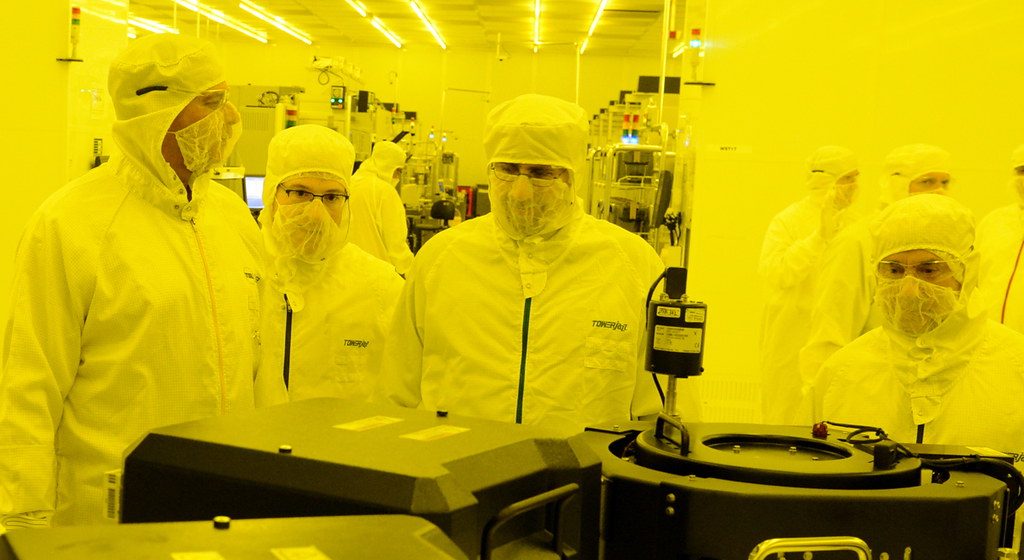
Key Partners and Institutions
This project brings together leading European research institutions and industry partners. The core participants include several renowned universities and research centers specializing in nanotechnology and semiconductor materials. Prominent industry players, including major semiconductor companies and technology startups, are also involved. This collaboration will leverage the combined expertise of academic researchers and industry practitioners to accelerate the project’s progress.
The collaboration is crucial for a successful transition from research to practical application.
Project Timeline and Phases
The project is structured in three distinct phases, each with specific milestones and deliverables. Phase 1 focuses on fundamental research and the development of novel nanomaterials. Phase 2 involves the design and prototyping of advanced semiconductor devices based on these nanomaterials. Phase 3 encompasses the scaling up of the technology and the establishment of pilot production lines.
The timeline for each phase is detailed in a comprehensive project plan. Each phase is expected to have a clear, measurable outcome.
Technological Advancements
This section delves into the innovative nanotechnologies central to the Europe Starts project for nanotechnology in semiconductors. It details the specific nanomaterials employed, their projected impact on semiconductor performance, and how they address existing limitations in the field. A comparison with existing methods, along with a table outlining potential improvements, is also included.The project envisions a significant leap forward in semiconductor fabrication by leveraging the unique properties of nanomaterials.
These materials, at the atomic and molecular level, exhibit extraordinary characteristics that traditional methods struggle to replicate. By integrating these advanced materials into the semiconductor manufacturing process, the project anticipates overcoming existing bottlenecks in performance, cost, and environmental impact.
Specific Nanotechnologies Employed
The project leverages several cutting-edge nanotechnologies. These include, but are not limited to, carbon nanotubes, graphene, and novel quantum dots. Each material possesses unique properties that can be harnessed for enhanced semiconductor performance. Carbon nanotubes, for instance, offer exceptional electrical conductivity, while graphene’s atomically thin structure enables high-speed electron transport. Quantum dots, with their tunable optical properties, promise advanced functionalities in optoelectronic devices.
Impact on Semiconductor Performance
The integration of these nanomaterials is expected to dramatically improve various semiconductor performance metrics. Enhanced electron mobility, reduced energy consumption, and improved signal processing are anticipated outcomes. Carbon nanotubes, with their exceptional conductivity, can enable faster switching speeds in transistors. Graphene, due to its high carrier mobility, is predicted to lead to faster and more energy-efficient integrated circuits.
Quantum dots, in turn, hold promise for higher efficiency in solar cells and light-emitting diodes. These advancements will contribute significantly to the development of next-generation electronics.
Comparison with Existing Methods
Current semiconductor manufacturing methods, while successful, face limitations in achieving the extreme miniaturization and performance enhancements envisioned by the project. Existing techniques, often based on silicon, struggle to maintain performance as feature sizes shrink. The proposed nanotechnologies offer a pathway to surpass these limitations, enabling the creation of devices with enhanced performance characteristics. For instance, carbon nanotubes can provide higher current densities than traditional silicon-based transistors, potentially allowing for smaller and faster transistors.
Overcoming Current Limitations
The project directly addresses current limitations in semiconductor technology by exploring alternative materials and fabrication techniques. The incorporation of nanomaterials promises to overcome scaling issues, improve performance, and reduce energy consumption. This shift from conventional materials to nanomaterials represents a significant paradigm shift in semiconductor manufacturing.
Table of Nanotechnologies and Potential Improvements
| Nanotechnology | Potential Improvement | Impact on Semiconductors | Challenges |
|---|---|---|---|
| Carbon Nanotubes | Enhanced conductivity and mechanical strength | Faster transistors, improved power efficiency | Scalability and cost-effectiveness in mass production |
| Graphene | High carrier mobility and flexibility | Faster integrated circuits, flexible displays | Challenges in large-scale transfer and integration |
| Quantum Dots | Tunable optical properties | Improved optoelectronic devices (e.g., LEDs, solar cells) | Control over size and uniformity in synthesis |
Economic Implications
The European Union’s commitment to nanotechnology in semiconductors promises significant economic benefits, fostering innovation and driving growth across various sectors. This initiative is poised to reshape the European technological landscape, attracting investment and creating high-skilled jobs. The project’s potential to enhance Europe’s global competitiveness in the semiconductor industry is substantial.The expected economic impact of this project extends beyond immediate gains, shaping Europe’s future technological leadership.
By investing in cutting-edge research and development, Europe can strengthen its position in the global semiconductor market and ensure long-term prosperity.
Projected Economic Impact
This project anticipates substantial economic returns. The development of advanced nanomaterials and semiconductor fabrication techniques will create a new market for European companies, leading to increased exports and enhanced competitiveness. This initiative can generate substantial revenue for companies specializing in semiconductor equipment, materials, and design.
Job Creation and Investment Opportunities
The project is expected to generate significant employment opportunities in high-tech fields. The creation of specialized research and development teams, fabrication facilities, and support industries will lead to a surge in employment opportunities. This project will also attract significant private investment in research and development, boosting economic growth. For instance, the development of new semiconductor manufacturing techniques could attract investments from global tech giants, creating spin-off companies and increasing overall employment.
Europe’s foray into nanotech for semiconductors is fascinating, but it’s worth noting the parallel challenges elsewhere. While European researchers are pushing the boundaries of miniaturization, spammers are targeting mobile phones in Asia, spammers target mobile phones in asia with increasingly sophisticated tactics. This highlights the complex interplay between technological advancement and its potential misuse, something that will likely influence the future of semiconductor development in Europe.
Market Value Estimation
Estimating the exact market value of the project’s outcomes is complex. However, the development of novel nanomaterials for semiconductors is likely to create a new market segment. A similar trajectory is observed in the development of new semiconductor materials and manufacturing techniques. The increased efficiency and performance of semiconductors resulting from nanotechnology applications are likely to result in increased demand and subsequently, market expansion.
The potential market value could be substantial, exceeding billions of Euros over the next decade.
Long-Term Benefits to Europe’s Technological Leadership
The project’s success will significantly contribute to Europe’s technological leadership in the semiconductor sector. The development of cutting-edge nanotechnology will give European companies a competitive advantage, fostering innovation and driving growth in related sectors. This initiative will ensure that Europe remains a key player in the global semiconductor industry, attracting top talent and promoting technological advancement. This can be seen in the current global semiconductor landscape where leadership in nanotechnology is becoming a crucial factor for competitiveness.
Investment in Research and Development
| Area | Estimated Investment (in millions of Euros) | Expected Return (in millions of Euros) |
|---|---|---|
| Nanomaterial Research and Development | 500 | 1500 |
| Advanced Semiconductor Fabrication | 750 | 2250 |
| Infrastructure Development and Support | 250 | 750 |
| Talent Acquisition and Training | 100 | 300 |
| Total Estimated Investment | 1600 | 4800 |
The table above presents a preliminary estimation of investment and expected returns. These figures are subject to change based on the actual project progress and market conditions. These figures provide a reasonable estimate of the potential investment and the projected economic benefits. Furthermore, the investment is crucial for securing Europe’s position in the high-tech sector.
Europe’s foray into nanotech for semiconductors is exciting, but the practical implications are still unfolding. Meanwhile, companies like Buy.com are offering legit music downloads, though with some restrictions, which is interesting in the context of the future of digital content. Buy.com debuts legit music downloads strings attached highlights the complexities of digital distribution. Ultimately, European nanotech advancements in semiconductors are poised to revolutionize the industry in ways we’re only beginning to grasp.
Societal Impact
This project promises significant societal benefits, extending far beyond the realm of advanced semiconductor technology. From job creation and educational opportunities to its influence on related industries and its contribution to sustainability, the ripple effects will be felt throughout Europe. Understanding these impacts is crucial for maximizing the project’s positive influence and mitigating potential challenges.The societal impact of this European nanotechnology project for semiconductors will be multifaceted, encompassing economic opportunities, educational advancements, and the potential for sustainable practices.
Careful consideration of ethical implications and their mitigation is paramount to ensure responsible development and implementation.
Potential Job Creation and Educational Opportunities
The project’s development of cutting-edge nanotechnology will necessitate a skilled workforce. This will create a significant number of high-skilled jobs in research, development, manufacturing, and maintenance. The need for specialized engineers, technicians, and scientists will drive demand in related fields, potentially fostering a virtuous cycle of economic growth. Furthermore, educational institutions will be challenged to adapt curricula to equip students with the necessary skills for these emerging roles.
Training programs and apprenticeships will play a crucial role in upskilling the existing workforce and attracting talent to these new fields.
Impact on Related Industries, Europe starts project for nanotech in semiconductors
The advancements in semiconductor technology will have a profound impact on industries reliant on these components. The electronics and telecommunications sectors stand to gain from improved performance, reduced costs, and enhanced functionalities. This will lead to new product development, increased efficiency, and potentially lower prices for consumers. Consequently, the ripple effect extends to industries like consumer electronics, automotive, and medical technology, boosting innovation and economic activity.
Ethical Considerations and Challenges
The development of new technologies often raises ethical considerations. Careful attention must be paid to issues like equitable access to the technology, potential misuse of the technology, and the potential displacement of workers. The project must consider the environmental impact of manufacturing processes and the potential for data security breaches. Transparency and public engagement are crucial for addressing these concerns.
Open dialogue and proactive engagement with stakeholders will be essential for mitigating potential risks and building trust.
Contribution to Sustainability in the Semiconductor Industry
This project can significantly contribute to sustainability in the semiconductor industry by focusing on environmentally friendly manufacturing processes. The project should prioritize the use of renewable energy, reduce water consumption, and minimize waste generation. Moreover, the development of more efficient and energy-saving semiconductors will have a positive impact on the wider economy and society, reducing energy consumption and carbon emissions.
Comparison of Societal Impacts with Other European Initiatives
| Initiative | Job Creation | Environmental Impact | Ethical Concerns |
|---|---|---|---|
| European Nanotech Project for Semiconductors | High potential for specialized jobs in R&D, manufacturing, and maintenance; upskilling of existing workforce needed. | Potential for reduced energy consumption and carbon emissions through more efficient semiconductors; focus on sustainable manufacturing practices. | Equitable access, potential misuse of technology, workforce displacement, data security concerns, environmental impact of manufacturing processes; requires careful consideration and mitigation strategies. |
| European Green Deal | Focus on green jobs and transition to a low-carbon economy; potential for job displacement in fossil fuel industries. | Significant emphasis on reducing emissions, transitioning to renewable energy, and promoting circular economy principles. | Potential social and economic disruptions associated with the transition; fair and just transition policies crucial. |
| Horizon Europe | Funding for various research projects across diverse fields; creates a wide spectrum of jobs and educational opportunities. | Promotes sustainable solutions across many research areas. | Balancing the need for innovation with the potential societal impact; ethical considerations related to specific research areas vary. |
International Context
Europe’s ambitious nanotechnology project for semiconductors is poised to reshape the global landscape. This initiative, while deeply rooted in European needs and priorities, cannot exist in isolation. Understanding the global context, comparing it with existing efforts, and identifying potential partnerships is crucial for its success. The project’s global implications are significant, with the potential to influence the future of semiconductor technology worldwide.
Comparative Analysis of Global Initiatives
The European project finds itself amidst a burgeoning global effort in nanotechnology. Many countries, recognizing the transformative potential of nanomaterials in semiconductors, are investing heavily in research and development. For example, the United States has a robust history of funding nanotechnology research, often focused on specific applications and materials. Asia, particularly South Korea and Japan, has made significant strides in semiconductor manufacturing and nanotechnology integration, often with a strong emphasis on commercialization.
Understanding the strengths and weaknesses of these different approaches will help the European project to find its niche and leverage global collaborations.
Europe’s foray into nanotechnology for semiconductors is fascinating. Imagine the possibilities, especially when coupled with advancements like those being explored by IBM’s Blue Gene supercomputer, which is now tackling the mysteries of the universe’s origins. IBM’s Blue Gene supercomputer to seek origins of universe This powerful tool could potentially unlock crucial insights into materials science, potentially accelerating the development of even smaller, faster, and more efficient semiconductor components.
Ultimately, this European nanotech project holds tremendous promise for the future of computing.
Competitive Landscape for Nanotechnology in Semiconductors
The semiconductor industry is fiercely competitive. Nanotechnology offers the potential to significantly enhance performance and efficiency, leading to new products and applications. Companies and research institutions worldwide are aggressively pursuing advancements in this field. The competitive landscape is not just about developing new materials; it also involves intellectual property protection, manufacturing processes, and ultimately, market share. This dynamic environment necessitates a strategic approach to ensure the European project remains competitive and innovative.
Potential Collaborations with Other Countries
Collaboration is essential for maximizing the impact of the European project. Partnerships with other nations can leverage diverse expertise and resources. Countries with strong nanotechnology capabilities, such as the United States, South Korea, or Japan, could be ideal partners. Joint research initiatives, technology transfer agreements, and shared infrastructure can accelerate progress. Such collaborations could lead to breakthroughs that would be unattainable through independent efforts.
Global Implications of the European Project
The European project’s success will have profound global implications. It could lead to new standards for semiconductor manufacturing, impacting industries ranging from consumer electronics to medical devices. The adoption of these technologies could spur economic growth and create new jobs globally. Additionally, the project could encourage a more coordinated approach to nanotechnology research and development, fostering a more collaborative global scientific community.
Key Similarities and Differences Between European and Global Projects
| Feature | European Project | Global Initiatives |
|---|---|---|
| Focus Area | Broader semiconductor applications, emphasizing sustainability and societal impact. | Diverse, ranging from specific materials to specific applications (e.g., energy, healthcare). |
| Funding Model | Combination of public and private funding, with emphasis on EU-wide cooperation. | Varying models, including government grants, venture capital, and corporate investment. |
| Governance Structure | European Union-centric, with a focus on coordination and harmonization. | Highly variable, ranging from national to multinational structures. |
| Target Market | European and global markets, aiming for leadership in specific sectors. | Diverse, ranging from national markets to global ones. |
| Technological Focus | Emphasis on advanced materials, device architectures, and manufacturing processes. | Focus on various materials, applications, and technologies for nanotechnology. |
Future Directions

The European nanotechnology project for semiconductors promises exciting advancements, but its true impact hinges on the forward-thinking research and strategic implementation of its findings. This section Artikels potential future research directions, anticipates potential breakthroughs, considers broader applications, and explores scaling up the project’s outcomes for maximum societal benefit.Future research should focus on exploring the intricate relationship between nanomaterial properties and device performance in semiconductors.
This necessitates investigating novel synthesis methods and characterization techniques to create materials with precise control over their structure and composition at the nanoscale.
Potential Research Directions
This project’s findings pave the way for several innovative research avenues. Further research should investigate the creation of highly efficient, low-power nanodevices. Exploring novel device architectures incorporating nanomaterials could lead to groundbreaking improvements in performance metrics, such as speed, power consumption, and memory density. Integration of nanomaterials with existing semiconductor technologies should also be explored to achieve seamless transitions and optimize functionalities.
Potential Breakthroughs in Nanotechnology
The project’s potential breakthroughs lie in its ability to engineer materials with tailored properties. For instance, controlling the quantum mechanical behavior of electrons at the nanoscale could lead to devices with unprecedented speed and efficiency. Furthermore, novel methods for assembling nanostructures into complex circuits could revolutionize computing capabilities. A deeper understanding of the interactions between nanomaterials and their environment could also open doors for more sustainable and environmentally friendly manufacturing processes.
Potential Applications in Other Sectors
The project’s findings aren’t confined to semiconductors. Nanomaterials’ unique properties could find applications in diverse sectors. For example, in medicine, nanodevices could enhance drug delivery systems, enabling more targeted therapies and minimizing side effects. In energy production, nanomaterials could improve the efficiency of solar cells and batteries. In environmental science, nanotechnologies could develop innovative solutions for water purification and pollution control.
Scaling Up Project Outcomes
To maximize the project’s impact, a collaborative approach is essential. Partnerships between research institutions, industry players, and government agencies are crucial for the successful transfer of knowledge and technologies. Creating dedicated infrastructure for nanomaterial synthesis and characterization will accelerate progress and attract talent. Clear intellectual property strategies and fostering a supportive regulatory environment will ensure that new technologies are developed and deployed responsibly.
Impact on the Future of Technology
“Nanotechnology holds the key to unlocking a future where technology is both powerful and responsible, pushing the boundaries of what is possible while addressing the challenges of our time. This project represents a crucial step in that journey.”
Ending Remarks
In conclusion, Europe’s commitment to nanotechnology in semiconductors signifies a significant step forward in technological innovation. This project promises substantial economic benefits, job creation, and advancements in sustainability. The project’s potential to reshape the future of semiconductor technology is substantial, and its global implications are considerable. We can anticipate a transformative impact on the industry and beyond, solidifying Europe’s position as a global leader in technological innovation.