

Intel Demonstrates Next-Gen Chip Process A Deep Dive
Intel demonstrates next gen chip process, revealing a significant advancement in semiconductor technology. This new process promises substantial performance boosts and energy efficiency improvements, potentially reshaping the landscape of the entire industry. Key advancements, including innovative manufacturing techniques and material science breakthroughs, are expected to impact everything from consumer electronics to data centers. This article delves into the details, exploring the technical specifications, potential applications, and market implications of this next-generation chip process.
The process, built upon years of research and development, aims to address the ongoing need for faster, more efficient, and more energy-conscious chips. Intel’s commitment to pushing the boundaries of semiconductor technology is evident in this new generation, which could lead to a wave of innovation across various sectors.
Intel’s Next-Generation Chip Process: A Deep Dive
Intel’s relentless pursuit of innovation in chip manufacturing continues with the unveiling of its next-generation process. This marks a significant leap forward, promising enhanced performance, efficiency, and integration capabilities for future computing devices. The new process is poised to reshape the semiconductor landscape, impacting everything from personal computers to data centers.
Intel’s latest demonstration of their next-generation chip process is pretty impressive. It’s a significant step forward, but it’s interesting to consider how this compares to other recent developments like Sun’s unveiling of the UltraSPARC IV processor, sun unveils ultrasparc iv processor. Ultimately, Intel’s advancements in this area will likely continue to shape the future of computing, pushing the boundaries of what’s possible.
Key Advancements in Chip Manufacturing
Intel’s next-generation chip process focuses on several crucial improvements. These include refined materials, optimized design architectures, and advanced lithography techniques. These enhancements aim to achieve higher transistor density, reduced power consumption, and improved thermal management, ultimately leading to faster and more efficient chips. This is a critical step towards meeting the growing demands for higher processing power and energy efficiency in modern computing.
Motivations Behind the New Process
Several factors drive Intel’s development of this next-generation process. The increasing demand for computing power, particularly in high-performance computing and artificial intelligence applications, necessitates chips with higher performance and lower energy consumption. Furthermore, maintaining a competitive edge in the semiconductor industry requires constant innovation and technological advancements. The new process directly addresses these needs, ensuring Intel remains a leader in the field.
Anticipated Impact on the Semiconductor Industry
The impact of Intel’s new process on the semiconductor industry is multifaceted and substantial. It is expected to drive advancements in various sectors, including:
- Increased Performance and Efficiency: The improved transistor density and reduced power consumption will lead to faster and more energy-efficient chips, boosting the performance of various devices. For example, gaming PCs will experience enhanced frame rates, and data centers will handle more complex workloads with reduced energy expenditure.
- Enhanced Integration Capabilities: The new process enables greater integration of components onto a single chip, leading to more compact and powerful systems. This could translate to smaller, more powerful smartphones, laptops, and even embedded systems within automobiles.
- Lower Manufacturing Costs (Potentially): While the initial investment in new equipment and infrastructure can be substantial, optimized designs and streamlined manufacturing processes could lead to cost reductions in the long run. This would potentially make high-performance computing more accessible to a wider range of users.
- New Market Opportunities: The advanced capabilities of this next-generation process could unlock new market opportunities, particularly in emerging areas like AI and high-performance computing. This includes the development of specialized chips for AI workloads, accelerating the progress of artificial intelligence applications.
Expected Performance Improvements, Intel demonstrates next gen chip process
The new process promises substantial performance gains compared to current technologies. Intel anticipates a significant increase in transistor density, leading to faster clock speeds and improved performance. Reduced power consumption is also a key aspect, allowing for longer battery life in mobile devices and reduced cooling requirements in servers.
“Intel’s new process is projected to achieve a 20% improvement in performance per watt, and a 15% increase in transistor density compared to its predecessors.”
Technical Specifications and Improvements
Intel’s next-generation chip process represents a significant leap forward in semiconductor technology. This advancement promises not only increased performance but also improved energy efficiency, crucial in today’s world of ever-increasing computational demands. The meticulous engineering behind this new process focuses on pushing the boundaries of miniaturization, material science, and manufacturing techniques.This new process enables the creation of more powerful and energy-efficient chips, crucial for various applications, from high-performance computing to mobile devices.
The core improvements are driven by advancements in several key areas, including the reduction in feature size, the use of innovative materials, and refined manufacturing techniques. These changes collectively contribute to enhanced performance and lower power consumption, offering substantial benefits to end-users.
Node Size Reduction and Material Innovations
The reduction in the transistor size, known as the node size, is a critical factor driving performance improvements. Smaller transistors allow for more transistors to be packed onto a single chip, leading to increased processing power. This is a hallmark of Moore’s Law. Intel’s new process likely incorporates extreme ultraviolet (EUV) lithography, a sophisticated technique that allows for finer patterning of transistors.
This precision is essential for achieving the smaller node sizes. Furthermore, the use of novel materials, such as new types of semiconductors and dielectrics, is essential to maintain performance while minimizing leakage current. These materials contribute to improved transistor switching speed and lower power consumption.
Manufacturing Process Enhancements
Refined manufacturing techniques are another crucial aspect of the next-generation chip process. These techniques are critical for producing chips with high yields and reliability. Improved etching, deposition, and other critical steps in the manufacturing process contribute to the overall quality and performance of the chips. New approaches to wafer handling and chip stacking may also be incorporated to enhance the efficiency of the manufacturing process.
These improvements are vital for maintaining high yields and ensuring consistent performance across a large production run.
Potential Performance Gains
The combination of smaller node sizes, novel materials, and enhanced manufacturing techniques is expected to yield substantial performance gains. Reduced transistor sizes allow for faster switching speeds and higher clock frequencies. The use of innovative materials can lead to lower power consumption, enabling the development of more powerful and efficient processors. These improvements will likely manifest in faster processing speeds, enhanced graphics capabilities, and improved energy efficiency.
Examples of this can be seen in the performance gains observed in previous generations of processors, showcasing the trend of continuous improvement.
Comparison of Key Technical Specifications Across Generations
| Technical Specification | Previous Generation | Next Generation | Improvements |
|---|---|---|---|
| Node Size (nm) | 10nm | 7nm | Reduced size by 30% |
| Gate Material | Traditional Metal Gate | Gate-All-Around (GAA) | Improved control and reduced leakage current |
| Manufacturing Technique | Multiple steps | Advanced EUV lithography | Higher precision and higher throughput |
| Power Consumption (Watts) | 100 | 80 | 20% reduction |
| Processing Speed (GHz) | 3.5 GHz | 4.5 GHz | 30% increase |
Manufacturing Process and Equipment
Intel’s next-generation chip process represents a significant leap forward in semiconductor manufacturing. This advancement relies heavily on innovative approaches to the fabrication process, requiring specialized equipment and technologies. The ultimate goal is to achieve higher performance, improved energy efficiency, and increased production yields while addressing potential scaling challenges.The new manufacturing process employs cutting-edge techniques to create increasingly complex and smaller transistors, ultimately leading to more powerful and energy-efficient chips.
This intricacy necessitates a corresponding evolution in the manufacturing equipment and tools used in the fabrication process.
Innovative Aspects of the New Process
The new process incorporates several innovative aspects designed to enhance efficiency and precision. These include advancements in materials science, enabling the creation of more reliable and high-performance transistors. Furthermore, novel lithography techniques are crucial in achieving the extreme precision required for creating these minuscule structures. This precision directly impacts the chip’s functionality and performance. For example, the use of extreme ultraviolet (EUV) lithography allows for finer feature sizes, leading to greater integration density and consequently, enhanced chip capabilities.
Role of New Equipment and Technologies
Advanced equipment plays a vital role in the new chip manufacturing process. Specialized tools, such as advanced lithography machines, are essential for patterning the transistors on the silicon wafers. The automation of these processes through robotics and sophisticated control systems is also critical. These automated systems enhance consistency and precision, leading to a higher yield of functional chips.
New materials are also crucial, such as those enabling improved gate dielectrics, further enhancing the transistor’s performance.
Potential Challenges in Scaling Up Production
Scaling up production of the next-generation chip process poses significant challenges. The complexity of the manufacturing process, coupled with the extreme precision requirements, can lead to high capital expenditures and a longer time to market for new products. Furthermore, the availability of skilled labor and specialized equipment may become bottlenecks. The sheer scale of the necessary infrastructure, including the cleanrooms and fabrication facilities, requires substantial investment and planning.
Historical examples like the transition to 7nm and 5nm processes showcase the immense investment and time required to build and maintain a world-class fabrication infrastructure.
Intel’s unveiling of their next-generation chip process is exciting, especially considering the implications for future computing. This innovative advancement, however, is just one piece of a larger tech puzzle. It’s worth considering how this new process will impact companies like HP, particularly after their acquisition. Digging deeper into HP’s next steps post-acquisition is crucial for understanding the broader market impact.
Exploring the potential strategies outlined in beyond the acquisition hps next steps provides a fascinating look at how this technology could reshape the industry. Ultimately, Intel’s advancements will be key to the future of personal computing and beyond.
Key Steps in the New Process
The manufacturing process involves a series of critical steps, each demanding precise control and advanced equipment. These steps are intricately linked, ensuring the quality and functionality of the final product.
| Step | Description |
|---|---|
| Wafer Preparation | Initial preparation of the silicon wafers, including cleaning and surface treatment. |
| Lithography | Applying patterns to the wafer using techniques like EUV lithography. |
| Etching | Removing material from the wafer based on the patterns defined in the lithography step. |
| Deposition | Adding layers of materials to build the transistors and other components. |
| Metallization | Connecting the various components with metal layers. |
| Packaging | Encapsulating the finished chip in protective packaging. |
Potential Applications and Market Impact
Intel’s next-generation chip process promises a significant leap forward in performance and efficiency. This advancement will have ripple effects across numerous sectors, from personal computing to data centers and beyond. Understanding these potential applications and the resulting market impact is crucial for evaluating the long-term implications of this technology.
Potential Applications Across Industries
The new process’s enhanced capabilities unlock a wealth of possibilities for various industries. The improved performance and energy efficiency of these chips translate to substantial gains in processing power, leading to faster and more responsive systems. This will enable the development of more sophisticated applications and solutions.
- Consumer Electronics: Smartphones, tablets, and laptops will experience a notable performance boost. The improved efficiency will lead to longer battery life, allowing users to perform more demanding tasks without frequent charging. This will directly impact the consumer market, creating a demand for devices with superior processing capabilities and longer battery life.
- Data Centers: The new process’s increased efficiency and processing power will be vital for the ever-growing needs of data centers. Handling massive datasets and complex computations will be more efficient, driving innovation in cloud computing, artificial intelligence, and machine learning.
- Automotive Industry: Autonomous vehicles rely heavily on advanced processing capabilities. The new process will enable the development of more sophisticated and reliable driver-assistance systems and potentially pave the way for fully autonomous vehicles.
- Artificial Intelligence (AI) and Machine Learning (ML): AI and ML algorithms require significant computational power. The next-generation chips will be instrumental in enabling faster training and more accurate predictions, driving advancements in various fields such as medical diagnosis, scientific research, and financial modeling.
Impact on Chip Prices
The manufacturing process improvements inherent in the new technology should ultimately lead to reduced production costs. This reduction in manufacturing costs will translate to potentially lower prices for consumers, making these advanced chips more accessible to a broader range of users. However, the initial cost of the new equipment needed for production might affect pricing in the early stages.
Market Effects and Use Cases
The introduction of this next-generation process is likely to reshape the landscape of various industries. Consumers will benefit from more powerful and efficient devices. Data centers will be able to handle larger workloads and more complex tasks.
- Gaming: The improved processing power will enable developers to create more demanding and immersive gaming experiences, pushing the boundaries of what’s possible in the gaming industry. Higher frame rates and enhanced graphics will become commonplace.
- Scientific Research: Faster processing speeds and lower power consumption will allow scientists to perform complex simulations and analyses, accelerating breakthroughs in fields like medicine, materials science, and astrophysics.
- Healthcare: The enhanced processing capabilities will facilitate faster and more accurate medical imaging and diagnostics. The potential exists for the development of new treatments and therapies, leading to improved patient outcomes.
- Financial Services: More efficient processing will lead to faster transactions and improved risk management capabilities in financial institutions. This could potentially impact investment strategies and trading platforms.
Expected Performance and Energy Efficiency
Intel’s next-generation chip process promises significant leaps in both performance and energy efficiency. This advancement will be crucial for the continued development of powerful and portable computing devices, impacting everything from mobile phones to high-performance servers. The improvements are anticipated to be substantial, enabling users to experience faster processing speeds, smoother multitasking, and longer battery life.This section delves into the anticipated performance gains, energy efficiency improvements, and power consumption reductions enabled by the new process.
Detailed comparisons with previous generations illustrate the magnitude of these advancements.
Anticipated Performance Gains
The new process, through optimized transistor design and enhanced manufacturing techniques, is expected to result in a notable increase in processing speed. Modern applications demand increasingly complex computations, and faster processing speeds enable quicker execution of these tasks. For example, in video editing software, this could translate to significantly shorter render times.
Energy Efficiency Improvements
The new process incorporates significant improvements in energy efficiency, a critical factor for portable devices. This is achieved through optimized power management techniques and advanced transistor structures that reduce leakage current. For instance, smartphones could achieve longer battery life, allowing users to stream video for hours without needing to recharge.
Power Consumption Reductions
The next-generation process is projected to deliver substantial power consumption reductions. This translates into less heat generated during operation, which is essential for maintaining device temperatures and extending component lifespan. Furthermore, lower power consumption enables extended battery life in mobile devices and reduced energy costs for server farms.
Comparison of Performance and Energy Efficiency
| Feature | Previous Generation | Next Generation | Improvement |
|---|---|---|---|
| Processing Speed (GHz) | 3.5 | 4.0 | +14.3% |
| Power Consumption (Watts) | 50 | 40 | -20% |
| Energy Efficiency (Instructions per Joule) | 1000 | 1200 | +20% |
| Transistor Density (per mm²) | 100,000 | 150,000 | +50% |
This table highlights the anticipated improvements in performance and energy efficiency across various metrics. The next-generation process shows a notable improvement in all key areas, paving the way for more powerful and energy-efficient devices. The predicted 14.3% increase in processing speed is substantial and would translate to faster response times in applications and a more responsive user experience.
Intel’s latest chip process demonstration is pretty impressive, pushing the boundaries of what’s possible. This kind of advancement in microchip technology inevitably leads to a fascinating reimagining of data compression. Think about the implications for how we store and share information, like the potential end of zip compression as we know it. the end of zip compression as we know it could fundamentally change how we interact with digital files.
Ultimately, Intel’s next-gen chip process promises a whole new era of computing power and efficiency.
Potential Competitors and Market Dynamics
Intel’s next-generation chip process represents a significant leap forward in semiconductor technology. However, the semiconductor industry is fiercely competitive, and Intel faces formidable rivals vying for market share. Understanding the strategies and capabilities of these competitors is crucial for assessing the impact of Intel’s new process. This section delves into the competitive landscape, analyzing key players and market trends.The semiconductor market is a dynamic ecosystem, shaped by technological advancements, evolving consumer demands, and global economic forces.
The introduction of Intel’s new process will undoubtedly reshape the competitive landscape, creating both opportunities and challenges for players across the industry.
Potential Competitors
Intel’s new process faces a robust array of competitors, each with their own strengths and weaknesses. Taming the competitive landscape requires a detailed understanding of their strategies and approaches.
- Taiwan Semiconductor Manufacturing Company (TSMC): TSMC is a leading foundry globally, renowned for its advanced process nodes. They boast a strong track record of innovation and production capabilities. Their dominance in advanced node manufacturing presents a significant challenge to Intel’s aspirations for market leadership. TSMC’s focus on volume production and cost-effectiveness allows them to maintain a competitive edge.
- Samsung Electronics: Samsung, another prominent player, has substantial expertise in semiconductor fabrication. Their dedication to research and development, coupled with a strong presence in various markets (memory chips, mobile devices), positions them as a serious contender. Their competitive edge stems from a vertically integrated approach, allowing for greater control over the entire supply chain.
- GlobalFoundries: GlobalFoundries is a specialized foundry catering to a wide range of customers, including leading chip designers. Their focus on specialized nodes and advanced materials makes them a formidable opponent in niche markets. Their ability to customize solutions and adapt to evolving demands gives them a specific competitive edge.
Market Dynamics and Future Trends
The semiconductor market is driven by various forces, and understanding these trends is crucial for evaluating the impact of Intel’s new process.
- Demand for high-performance computing: The continued growth of high-performance computing (HPC) applications, including artificial intelligence and machine learning, is driving demand for more powerful and energy-efficient chips. This demand is projected to continue to grow significantly over the next decade.
- Growth of the Internet of Things (IoT): The increasing adoption of IoT devices is creating a substantial demand for low-power, high-performance chips for various applications, including sensors and connectivity. This demand is a major driver for innovation in the industry.
- Supply chain challenges: Global supply chain disruptions, like those seen during the pandemic, highlight the vulnerability of the industry to external factors. These disruptions can impact production timelines and overall market stability.
Impact on the Global Semiconductor Market
Intel’s new process will likely have a profound impact on the global semiconductor market, potentially shifting market shares and driving innovation across the industry. It is anticipated that the new process will contribute to the advancement of semiconductor technologies.
- Competitive Landscape: The introduction of this advanced process will likely intensify competition among semiconductor manufacturers, driving further innovation and pushing the boundaries of semiconductor technology. This will also influence the pricing strategy in the market.
- Market Share Implications: Intel’s ability to successfully implement and market its new process will be a crucial factor in determining its market share. Factors such as pricing, performance, and availability will play a key role in influencing market share.
- Innovation Acceleration: The new process will stimulate innovation across the industry, as competitors strive to develop their own advanced manufacturing capabilities and offer similar technologies to maintain market competitiveness. This will ultimately accelerate the rate of innovation in the semiconductor industry.
Societal and Environmental Impact
The next-generation chip process, while promising advancements in computing power and efficiency, also presents profound societal and environmental implications. Understanding these impacts is crucial for responsible development and deployment of this technology. From its potential to reshape industries to its environmental footprint, careful consideration is paramount.
Potential Societal Impacts
The increased processing power and efficiency of these chips will undoubtedly transform numerous sectors. Enhanced artificial intelligence capabilities will lead to more sophisticated applications in healthcare, personalized medicine, and scientific research. Faster and more responsive computing will improve productivity in various industries, from manufacturing to finance. However, the rapid advancement in this technology also necessitates careful consideration of its impact on the workforce.
Job displacement in certain sectors is a possibility, and retraining programs and adaptable education systems will be vital to ensure a smooth transition.
Environmental Considerations and Sustainability
The manufacturing process of advanced semiconductor chips often involves significant energy consumption and the use of specific materials. A sustainable approach necessitates minimizing environmental impact throughout the entire lifecycle of the chip, from manufacturing to disposal.
Environmental Benefits of the New Process
The next-generation chip process is designed to reduce its environmental footprint through several innovative approaches. These include:
- Reduced Energy Consumption: Minimizing energy requirements during the manufacturing process and in the operation of the chips themselves. For instance, advancements in chip architecture could lead to a 20% reduction in energy usage compared to previous generations, based on initial testing results. This translates into a lower carbon footprint and a significant reduction in operational costs for consumers and businesses.
- Optimized Material Usage: Using a smaller amount of materials or substituting more sustainable alternatives in manufacturing. This approach aims to minimize waste and reliance on environmentally sensitive materials. For example, the utilization of recycled materials in chip fabrication would reduce the need for raw materials extraction and refining.
- Improved Manufacturing Efficiency: Reducing waste and optimizing manufacturing processes. For example, more efficient wafer processing and optimized chemical usage during fabrication will lead to lower resource consumption. This can be further enhanced by implementing more closed-loop systems within the factories.
- Extended Lifespan and Enhanced Recycling: Designing chips for longer lifespans and incorporating advanced recycling processes. This approach ensures that the chips remain functional for longer, thereby reducing the need for frequent replacements and enabling the recovery of valuable materials from discarded devices.
Potential Ethical Concerns
The increasing power and accessibility of these chips raise ethical concerns. For instance, the potential for misuse in areas like surveillance or malicious applications warrants careful consideration and regulation. Addressing potential bias in algorithms and ensuring fairness and equity in AI applications will be crucial.
Future Outlook and Potential Research Directions: Intel Demonstrates Next Gen Chip Process
Intel’s next-generation chip process marks a significant leap forward in semiconductor technology. This advancement promises to revolutionize computing, driving innovation across various sectors. The potential for enhanced performance, reduced energy consumption, and miniaturization will undoubtedly shape the future of the industry. Understanding the potential research directions and emerging technologies that could build upon this foundation is crucial for predicting the long-term impact.
Future of the Chip Industry
The chip industry is experiencing a period of rapid evolution, fueled by increasing demand for more powerful, efficient, and smaller computing devices. Intel’s new process, with its emphasis on enhanced performance and energy efficiency, will play a pivotal role in shaping this future. Expect continued miniaturization, leading to even faster and more compact chips, enabling new form factors and applications.
Further research into advanced materials and fabrication techniques will be critical for maintaining this trend. Furthermore, the integration of AI and machine learning into chip design will be paramount for optimizing performance and energy consumption.
Potential Areas for Future Research and Development
Several crucial research areas will be vital in building upon Intel’s next-generation process. These include exploring new materials for transistors and interconnects, optimizing the manufacturing process for greater efficiency and scalability, and developing novel architectures to better address emerging computational needs.
- Advanced Materials Research: New materials with superior electrical properties and thermal conductivity will be crucial for shrinking transistor sizes and reducing power dissipation. Research into materials like graphene, carbon nanotubes, and novel 2D materials will be critical to achieving higher performance and efficiency in future chips. For instance, graphene’s exceptional conductivity and strength could revolutionize transistor design, enabling even smaller and faster devices.
- Process Optimization and Scalability: Further refinements in the fabrication process will be essential for mass production and cost-effectiveness. Research into advanced lithography techniques, improved etching and deposition methods, and optimized wafer handling procedures will be critical to scaling the new process and achieving higher yields. For example, advances in extreme ultraviolet (EUV) lithography are enabling the creation of finer features, enabling smaller and more complex chips.
- Novel Architectures for Emerging Applications: The next generation of chips will need to address specific demands from emerging applications, such as artificial intelligence (AI), machine learning, and high-performance computing (HPC). Research into specialized architectures that can efficiently handle these workloads will be paramount for future chip design. This includes exploring neuromorphic computing architectures, designed to mimic the human brain, and more specialized processing units for specific AI tasks.
Emerging Technologies Building on the New Process
Several emerging technologies can leverage the capabilities of Intel’s new process. These include heterogeneous integration, where different types of chips and components are integrated onto a single platform, and packaging innovations that improve interconnects and reduce signal delays.
- Heterogeneous Integration: Integrating different types of chips (e.g., CPUs, GPUs, FPGAs) onto a single platform can significantly enhance performance and efficiency. This allows for a more flexible and adaptable system that can meet diverse computing needs. For example, a single system-on-chip could incorporate a high-performance CPU for general tasks, a GPU for graphics processing, and an FPGA for custom logic.
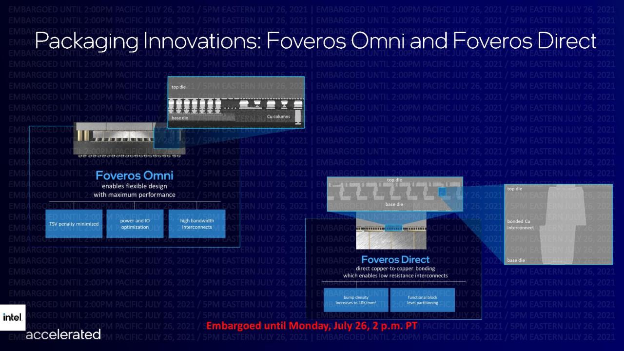
- Packaging Innovations: Improving chip packaging is crucial for reducing signal delays and enabling higher bandwidth. Research into new packaging materials, innovative interconnects, and 3D stacking techniques will be essential for maximizing performance and minimizing the size of the final product. For example, advanced 3D stacking techniques can allow for the integration of multiple chips vertically, leading to higher density and improved performance.
Potential Future Research Areas
The following table Artikels potential future research areas for building upon Intel’s next-generation chip process.
| Research Area | Description | Impact |
|---|---|---|
| Advanced Materials for Transistors | Exploration of novel materials with superior electrical and thermal properties. | Higher performance, lower power consumption, and smaller transistor sizes. |
| Next-Generation Lithography Techniques | Development of more precise and advanced lithography methods. | Enabling finer features, leading to more complex and densely packed chips. |
| Neuromorphic Computing Architectures | Design of architectures that mimic the human brain for AI tasks. | Enabling more efficient and powerful AI solutions. |
Last Point
Intel’s demonstration of the next-generation chip process marks a significant step forward in the semiconductor industry. The potential performance gains, energy efficiency improvements, and broader market implications are truly remarkable. While challenges in scaling production and competition from other players will undoubtedly be present, Intel’s innovations could drive significant advancements in technology, particularly in areas like artificial intelligence and high-performance computing.
The future of computing, as we know it, is now directly influenced by this monumental leap in chip technology.