

Material Thin as an Atom Tiniest Transistor
Material thin as an atom makes tiniest transistor, ushering in a new era of miniaturization in electronics. Transistors, the tiny switches that power our digital world, are constantly being shrunk. Current transistor technology is reaching its physical limits, demanding innovative solutions. This exploration dives deep into the fascinating world of atomically thin materials, examining their unique properties and potential to revolutionize transistor design.
This exciting new frontier promises faster, more energy-efficient, and smaller devices. Imagine the implications for everything from smartphones to supercomputers. We’ll delve into the science behind these advancements, discussing the properties of these materials, the manufacturing challenges, and the potential applications. We’ll also analyze the challenges and the exciting future directions of this groundbreaking technology.
Introduction to Atomic-Scale Transistors
Transistors are the fundamental building blocks of modern electronics, controlling the flow of electrical current and enabling the vast array of devices we use daily. From smartphones to supercomputers, these tiny switches are crucial for processing information and performing calculations. Miniaturization has been a driving force in electronics, leading to ever-smaller and more powerful devices. However, conventional transistor designs face limitations in terms of size and power consumption.
The quest for even faster, more energy-efficient electronics necessitates exploring new approaches, including the exciting prospect of atomic-scale transistors. These tiny devices, constructed from materials just a few atoms thick, promise to revolutionize the field by pushing the boundaries of miniaturization.The relentless pursuit of smaller, faster, and more energy-efficient electronics has driven a constant push for miniaturization. This trend is vital because smaller devices mean more complex circuits can be integrated into the same space, leading to enhanced performance and functionalities.
Current transistor technology, however, is approaching physical limitations. As transistors shrink, quantum effects become increasingly significant, impacting their performance. Heat dissipation becomes a critical challenge, and the intricate fabrication processes required for conventional transistors become progressively more complex and expensive. This motivates the exploration of new materials and designs, with atomic-scale transistors offering a promising avenue for overcoming these limitations.
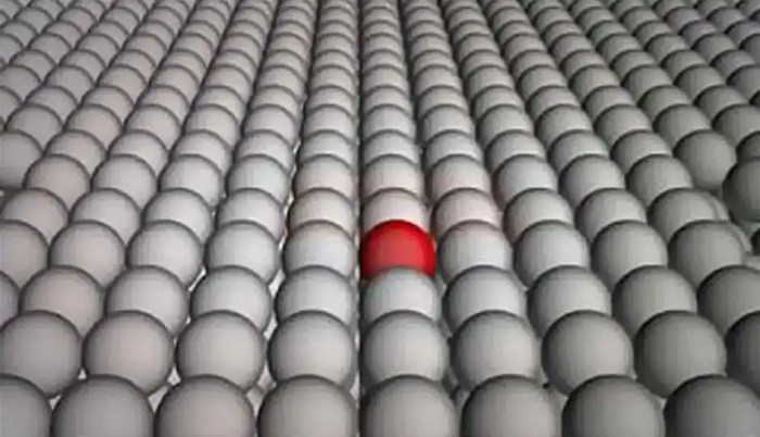
The unique properties of materials just a few atoms thick offer significant potential for achieving unprecedented miniaturization and performance.
Atomic-Scale Transistor Design
The design of atomic-scale transistors leverages the quantum mechanical properties of materials at the atomic level. These transistors use materials arranged with precise atomic precision, enabling control over the flow of electrons with unparalleled precision. This approach, in contrast to traditional techniques, exploits the behavior of electrons at the atomic level, enabling the creation of smaller and more energy-efficient transistors.
This allows for the creation of circuits with a vastly increased density of components, ultimately leading to more powerful and versatile devices.
Comparison of Traditional and Atomic-Scale Transistors
The table below highlights a comparison between traditional and atomic-scale transistors, illustrating the potential benefits of the latter.
| Transistor type | Material | Size | Power consumption |
|---|---|---|---|
| Traditional MOSFET | Silicon | ~100 nm | Moderate |
| Atomic-scale MOSFET | Graphene, MoS2, or other 2D materials | ~1 nm | Low |
The table illustrates that atomic-scale transistors, leveraging novel materials, can achieve significantly smaller dimensions and potentially lower power consumption compared to their traditional counterparts. The implications for the future of electronics are profound, promising devices that are smaller, faster, and more energy-efficient.
Properties of Atomically Thin Materials
Atomically thin materials, like graphene and molybdenum disulfide, possess extraordinary properties that distinguish them from their bulk counterparts. These two-dimensional structures exhibit unique electrical, mechanical, and thermal characteristics, promising revolutionary applications in electronics, energy, and other fields. Understanding these properties is crucial for harnessing their potential.Atomically thin materials, often referred to as 2D materials, differ fundamentally from their bulk counterparts due to their reduced dimensionality.
This reduction significantly alters their electronic, mechanical, and thermal behavior, leading to unique and potentially advantageous properties. The interactions between atoms in these materials are significantly different from those in bulk materials, resulting in distinct responses to external stimuli.
Electrical Properties
Atomically thin materials exhibit remarkable electrical conductivity. This is particularly evident in graphene, which displays exceptional electron mobility, exceeding that of many metals. The unique electronic band structure of these materials can be tailored to achieve specific electrical properties, making them suitable for various electronic applications. For example, the controlled doping of these materials can lead to n-type or p-type conductivity, essential for building transistors and other electronic components.
The tunability of their electrical properties through various techniques, like chemical doping or external electric fields, allows for intricate control over device performance.
Mechanical Properties
The mechanical properties of atomically thin materials are also exceptional. Graphene, for instance, possesses an exceptionally high tensile strength, exceeding that of many steel alloys. This extraordinary strength arises from the strong covalent bonds between carbon atoms in the hexagonal lattice structure. These materials’ flexibility and ability to withstand significant deformation make them suitable for flexible electronics and sensors.
The strength-to-weight ratio of these materials is remarkably high, offering potential for lightweight structural applications.
Thermal Properties
Thermal conductivity is another key property of atomically thin materials. These materials often display unique thermal transport characteristics. For instance, graphene exhibits exceptionally high thermal conductivity in the plane, enabling rapid heat dissipation. This property is crucial for preventing overheating in electronic devices, which can lead to performance degradation or failure. Conversely, some atomically thin materials exhibit low thermal conductivity in specific directions, making them suitable for thermal insulation.
Scientists are creating transistors unbelievably small, thinner than an atom! This groundbreaking material science is paving the way for incredibly powerful devices. Imagine a future where searching the internet is as simple as one tap – like the upcoming Motorola smartphone feature, allowing one-click Google searches. motorola smartphone to offer one click google search This innovation, combined with the miniaturization of transistors, hints at a new era of computing power and efficiency.
This dual behavior is a significant advantage.
| Material | Thermal Conductivity (W/mK) |
|---|---|
| Copper (Bulk) | 400 |
| Graphene | 5000 |
| Molybdenum Disulfide (MoS2) | 100 |
| Silicon (Bulk) | 150 |
The table above provides a comparison of the thermal conductivity of various materials, showcasing the remarkable thermal conductivity of graphene compared to bulk materials. The thermal conductivity of these materials can vary depending on the specific material and the direction of heat flow. This characteristic is crucial for designing efficient heat dissipation systems in electronic devices.
Advantages of Atomically Thin Materials in Electronics
Atomically thin materials offer several advantages in electronics. Their exceptional electrical, mechanical, and thermal properties make them promising candidates for high-performance transistors, flexible displays, and sensors. Their small size enables the creation of extremely compact and efficient devices. The tunability of their properties through various methods offers greater control over device characteristics.
Disadvantages of Atomically Thin Materials in Electronics
Despite their remarkable properties, atomically thin materials also present some challenges. Producing large-scale, high-quality samples can be challenging. The fabrication techniques are still under development, requiring further research and refinement. The integration of atomically thin materials with existing semiconductor technologies needs further investigation. The cost-effectiveness of large-scale production is a key factor to consider.
Manufacturing and Fabrication

Creating transistors at the atomic level presents a unique set of challenges, requiring precise control over materials at the smallest scales. The fabrication process is critical to realizing the potential of these devices, enabling their miniaturization and performance enhancement. Methods for producing atomically thin materials and integrating them into functional transistors are constantly evolving, pushing the boundaries of nanotechnology.
Methods for Creating Atomically Thin Materials
Producing materials thin enough to be considered “atomically thin” requires advanced techniques that manipulate materials at the nanoscale. These techniques are crucial for achieving the desired properties and functionalities in atomically thin transistors. A few prominent methods include:
- Mechanical exfoliation: This method, often likened to peeling layers of an onion, involves using adhesive tape to mechanically separate layers from a bulk crystal. This approach is relatively straightforward and has been instrumental in initial explorations of atomically thin materials. While effective for certain materials, it’s limited in terms of scalability and control over the size and quality of the obtained flakes.
- Chemical Vapor Deposition (CVD): CVD methods deposit atoms or molecules onto a substrate to create thin films. This approach allows for precise control over the composition and thickness of the resulting materials. However, achieving atomically thin layers with CVD can be challenging and often requires careful optimization of growth conditions. Variations of CVD, such as plasma-enhanced CVD, are also employed to improve control and uniformity.
- Epitaxy: Epitaxy involves growing a single crystal material layer-by-layer on a substrate with a specific crystal structure. This method offers precise control over the material’s structure and properties, which is critical for achieving the desired functionalities. The choice of substrate and growth parameters is essential to achieve the desired atomic thinness.
Challenges in Fabricating Atomically Thin Transistors
Several obstacles hinder the practical fabrication of transistors from atomically thin materials. These include:
- Maintaining material integrity: Atomically thin materials are extremely fragile and susceptible to damage during the fabrication process. Protecting these materials and ensuring their structural integrity throughout the fabrication process is a significant challenge. The transfer of atomically thin materials to substrates without introducing defects or wrinkles is crucial.
- Precise device patterning: Creating complex transistor structures with atomically thin materials demands high-resolution lithographic techniques. The challenge lies in creating the intricate patterns required for transistor operation with sufficient precision and control.
- Contacting atomically thin materials: Making electrical contacts to atomically thin materials is a crucial step. This is challenging due to the material’s fragility and the need to maintain the integrity of the material during contact formation. High-quality contacts are essential for reliable operation.
Procedure for Producing Graphene
Graphene, a well-known atomically thin material, can be produced using mechanical exfoliation. Here’s a simplified procedure:
- Substrate preparation: A highly oriented pyrolytic graphite (HOPG) single crystal is used as the source material. The HOPG crystal is carefully selected to ensure a high-quality surface.
- Exfoliation: A piece of Scotch tape is carefully placed on the HOPG crystal. The tape is then peeled off, transferring a layer of graphene to the tape. This process is repeated several times to obtain multiple graphene flakes. The tape is then carefully placed on a desired substrate to transfer the graphene.
- Transfer and characterization: The graphene flakes on the tape are transferred to a desired substrate. This is a critical step, as care must be taken to avoid damaging the graphene. The quality of the transferred graphene is assessed using various techniques, such as optical microscopy and Raman spectroscopy.
- Characterization: The produced graphene is analyzed using Raman spectroscopy to assess its quality and confirm the presence of defects. Further analysis such as atomic force microscopy or electron microscopy may be employed to gain insights into the structure and characteristics of the graphene.
Table of Fabrication Methods for Atomically Thin Transistors
| Fabrication Method | Material | Challenges | Solutions |
|---|---|---|---|
| Mechanical Exfoliation | Graphene, MoS2 | Scalability, material quality, transfer | Optimization of exfoliation process, advanced transfer techniques |
| Chemical Vapor Deposition (CVD) | Graphene, MoS2, others | Control over thickness, uniformity | Precise control of growth parameters, optimization of CVD process |
| Epitaxy | Various 2D materials | Substrate compatibility, growth control | Suitable substrate selection, advanced growth techniques |
Transistor Design and Functionality
Atomically thin materials, with their unique electronic properties, are revolutionizing transistor design. These materials, thinner than a single atom, enable the creation of transistors with unprecedented performance capabilities. Their exceptional control over electron flow promises faster speeds and lower power consumption, paving the way for more powerful and energy-efficient electronic devices.Different designs for transistors leverage the distinct properties of atomically thin materials.
Scientists are creating transistors incredibly small, thinner than an atom! This groundbreaking material innovation has huge implications for future tech. It’s a fascinating race to see who can make the smallest transistors, and this advancement is a significant leap forward. Looking at the historical context of the tech industry, figures like Bill Gates and Steve Jobs, and companies like Dell, Sony, HP, and even Wal Mart have shaped the tech landscape.
To learn more about the historical context of tech giants, check out this fascinating analysis: bill gates vs steve jobs dell does sony hp powers wal mart. Ultimately, these advancements in material science will drive even smaller and more powerful devices in the future.
These materials, often exhibiting exceptional conductivity or insulating properties, allow for precise control over the flow of electrons, leading to novel transistor architectures. The ability to manipulate the material at the atomic level unlocks a new frontier in miniaturization and performance enhancement.
Field-Effect Transistors (FETs)
FETs, a common transistor type, are being redesigned using atomically thin materials. These materials, such as graphene and molybdenum disulfide, exhibit exceptional electron mobility, which translates to faster switching speeds and reduced power consumption in the transistors. Gate dielectrics, crucial components of FETs, can be engineered with atomic precision, further enhancing performance. By integrating these materials, FETs show a remarkable improvement in power efficiency and speed compared to traditional silicon-based transistors.
Tunnel Field-Effect Transistors (TFETs)
TFETs are another promising type of transistor leveraging atomically thin materials. These transistors rely on quantum mechanical tunneling, allowing for extremely low power consumption. Materials like graphene and hexagonal boron nitride, known for their unique band structures, enable efficient tunneling, leading to transistors with significantly lower leakage currents and reduced power dissipation. This advancement in TFET design holds great potential for ultra-low power electronic systems.
Tunnel Junction Transistors (TJTs)
TJTs utilize tunneling phenomena to control current flow. Atomically thin materials, with their precise control over atomic structure, can be used to engineer the tunnel junction in TJTs, leading to enhanced performance characteristics. Materials like transition metal dichalcogenides (TMDCs) demonstrate excellent tunneling properties, making them ideal candidates for TJTs. This design promises to achieve even lower power consumption and faster switching speeds.
Performance Comparison of Transistor Types
| Transistor Type | Material | Switching Speed (ps) | Power Consumption (pJ) | Leakage Current (nA) |
|---|---|---|---|---|
| Silicon-based FET | Silicon | 100-500 | 10-50 | 1-10 |
| Graphene FET | Graphene | 10-100 | 1-10 | 0.1-1 |
| MoS2 FET | Molybdenum disulfide | 50-200 | 2-15 | 0.5-5 |
| Graphene TFET | Graphene | 5-50 | 0.1-5 | 0.01-0.5 |
| TMDC TJT | Transition metal dichalcogenide | 1-20 | 0.01-1 | 0.001-0.1 |
Note: Values are approximate and can vary based on specific device architecture and fabrication techniques.
Applications and Potential Impacts
Atomically thin transistors, with their unprecedented size and unique properties, promise a revolution across numerous technological sectors. These miniature marvels, built from materials just a few atoms thick, open doors to previously unimaginable performance improvements in computing, sensing, and energy management. Their potential impact on industries ranging from consumer electronics to healthcare is profound, promising advancements that were once the stuff of science fiction.
Potential Applications in Computing
Atomically thin transistors, with their exceptional speed and energy efficiency, can significantly enhance the performance of modern computers. Their ability to operate at extremely low voltages, coupled with their tiny size, leads to faster processing speeds and lower power consumption. This translates to more powerful and efficient laptops, smartphones, and supercomputers. For example, a significant reduction in energy consumption for a high-performance computer could lead to significant cost savings for businesses and universities.
Impact on Consumer Electronics
The integration of atomically thin transistors into consumer electronics promises a leap forward in performance and efficiency. Imagine smartphones with blazing-fast processing speeds, capable of handling complex tasks without overheating. Laptops and tablets could achieve similar performance gains, while maintaining their portability. This leads to enhanced user experiences and potentially even more affordable high-performance devices.
Applications in Sensors and Healthcare
The unique electrical properties of atomically thin materials make them ideal candidates for developing highly sensitive sensors. These transistors can detect minute changes in pressure, temperature, or chemical composition, with applications in environmental monitoring, medical diagnostics, and industrial process control. In healthcare, these sensors could lead to more accurate and rapid diagnostics, enabling early disease detection and personalized treatment plans.
Applications in Energy Storage
Atomically thin materials are also promising for advancements in energy storage. Their unique electronic structures can be engineered to improve the performance of batteries and supercapacitors. This translates to more efficient energy storage, longer battery life in portable devices, and potentially even advancements in electric vehicles. For example, thinner electrode materials in batteries can lead to faster charging times and greater energy density.
Potential Applications Across Industries, Material thin as an atom makes tiniest transistor
| Industry | Potential Application | Projected Benefits |
|---|---|---|
| Consumer Electronics | Faster processors, more energy-efficient devices | Enhanced user experience, lower operating costs |
| Healthcare | Highly sensitive biosensors, faster diagnostics | Improved disease detection, personalized medicine |
| Communications | More efficient and reliable wireless communication | Faster data transmission, lower latency |
| Aerospace | More efficient and reliable sensors for navigation and control | Enhanced safety and performance of aircraft and spacecraft |
| Automotive | Advanced sensors for autonomous driving, more efficient energy storage | Enhanced safety and performance of vehicles, reduced emissions |
Challenges and Future Directions
Atomically thin transistors, while promising, face several hurdles before widespread adoption. These challenges stem from the very nature of working at such a minuscule scale, demanding precise control and novel fabrication techniques. Overcoming these obstacles will be crucial for realizing the full potential of these groundbreaking devices.
Major Challenges in Development
The fabrication of atomically thin transistors presents significant hurdles. Maintaining the integrity of the atomically thin material throughout the manufacturing process is paramount. Imperfections, even at the atomic level, can drastically impact the device’s performance. Controlling the precise placement and arrangement of atoms during fabrication is another major challenge. This demands highly advanced techniques that can manipulate individual atoms or molecules with unparalleled precision.
Furthermore, achieving high-yield manufacturing is crucial for cost-effectiveness. The complexity of the fabrication process often leads to low yields, requiring significant improvements in process control.
Potential Solutions
Several approaches are being explored to address these challenges. Utilizing advanced materials with improved stability and mechanical properties can help maintain the integrity of the atomically thin layer during fabrication. Techniques such as molecular beam epitaxy (MBE) and chemical vapor deposition (CVD) are being refined to achieve higher precision in atom placement. Developing innovative lithographic techniques, perhaps incorporating advanced scanning probe microscopy (SPM) methods, will be essential for controlling the precise placement of atoms and molecules.
Moreover, automating and optimizing fabrication processes are crucial to increase yield and reduce production costs.
Future Research Directions
Future research should focus on exploring novel materials with enhanced electrical properties and stability. This could include incorporating two-dimensional materials with unique functionalities or developing hybrid structures combining atomically thin materials with other materials. Research into new device architectures is essential for achieving better performance and functionality. Investigating novel ways to integrate atomically thin transistors into existing electronic circuits and systems will be crucial for successful implementation.
Scientists are making transistors incredibly small, using materials thin as an atom. This breakthrough is amazing, but it’s not just about the physical size; it’s also about user control in the digital realm. For instance, yahoo mindset gives users control over search results , allowing more personalized and relevant searches. Ultimately, these advancements in both materials science and user experience are driving the future of computing and improving our digital lives, pushing the limits of what’s possible with transistors thinner than an atom.
Advanced characterization techniques to monitor the atomic-scale structure and properties of these devices throughout the manufacturing process are also crucial for understanding and mitigating defects.
Ongoing Research Projects
Several research groups worldwide are actively pursuing projects related to atomically thin transistors. A notable example is the development of graphene-based transistors at various institutions. Other projects involve exploring other two-dimensional materials, such as transition metal dichalcogenides (TMDs), to enhance device performance.
| Research Institution | Focus Area |
|---|---|
| University of California, Berkeley | Graphene-based transistor optimization |
| Massachusetts Institute of Technology | TMD transistor fabrication and characterization |
| Stanford University | Hybrid structures for enhanced performance |
These ongoing projects highlight the active research community exploring the potential of atomically thin transistors. The collaborations and knowledge sharing between these groups are essential for accelerating progress in this field.
Illustrative Examples: Material Thin As An Atom Makes Tiniest Transistor
Atomically thin materials, with their unique properties, are poised to revolutionize transistor technology. Their exceptional electrical conductivity, coupled with their ability to be precisely manipulated at the atomic level, opens doors to smaller, faster, and more energy-efficient transistors. This section will explore a specific example, focusing on molybdenum disulfide (MoS 2), a promising material for next-generation transistors.
Molybdenum Disulfide (MoS2) Transistors
Molybdenum disulfide (MoS 2) is a layered transition metal dichalcogenide (TMD). Its atomically thin structure, consisting of tightly bound sulfur and molybdenum atoms arranged in a honeycomb lattice, endows it with fascinating electrical and optical properties. The layered structure allows for easy exfoliation, enabling the creation of high-quality atomically thin films.
Unique Properties of MoS2
MoS 2 exhibits remarkable properties, making it suitable for transistor applications. Its direct band gap allows for efficient charge carrier transport, essential for transistor functionality. Furthermore, its high carrier mobility, meaning electrons move freely within the material, results in faster switching speeds compared to traditional silicon-based transistors. The material also demonstrates excellent chemical stability in various environments, crucial for long-term device reliability.
Fabrication Process of MoS2 Transistors
The fabrication process for MoS 2 transistors involves several key steps. First, high-quality MoS 2 crystals are exfoliated into atomically thin layers using techniques like mechanical exfoliation. Then, these layers are transferred onto a suitable substrate, often silicon or sapphire. Next, source and drain electrodes are patterned using lithography techniques. Finally, a gate dielectric layer is deposited, followed by the creation of a gate electrode, completing the transistor structure.
This precise control over the material’s placement and electrode geometry is vital for achieving desired transistor characteristics.
Demonstration of Advancement
The fabrication of MoS 2 transistors represents a significant advancement in transistor technology. By leveraging the unique properties of MoS 2, researchers can create transistors with significantly improved performance compared to traditional silicon transistors. These transistors exhibit faster switching speeds and potentially lower power consumption, paving the way for more efficient electronic devices.
Applications of MoS2 Transistors
MoS 2 transistors hold immense potential across various applications. Their high-speed operation makes them suitable for high-frequency circuits, enabling faster data processing. Their potential for low-power operation positions them as a candidate for low-power, portable electronic devices. Moreover, their ability to operate at high temperatures opens doors to specialized applications requiring robust performance in extreme conditions.
Structure of MoS2 Transistor
The structure of a MoS 2 transistor consists of a few layers of MoS 2 (typically 1-5 layers). A schematic representation would show a substrate (e.g., silicon), on which the MoS 2 layers are precisely positioned. Source and drain electrodes are connected to the MoS 2 layer, while a gate electrode sits above the MoS 2, separated by a thin gate dielectric layer.
The crucial feature is the atomically thin MoS 2 layer sandwiched between the electrodes. The thickness of the MoS 2 layer is typically measured in angstroms, highlighting the nanoscale nature of these devices.
| Feature | Description | Dimension (approximate) |
|---|---|---|
| MoS2 Layer | Atomically thin layer of molybdenum disulfide | 1-5 atomic layers |
| Substrate | Material supporting the MoS2 layer | Few hundred nanometers |
| Source/Drain Electrodes | Metal contacts for current flow | Tens of nanometers |
| Gate Dielectric | Insulating layer separating gate from MoS2 | Few nanometers |
| Gate Electrode | Electrode controlling the transistor’s conductivity | Tens of nanometers |
Concluding Remarks
In conclusion, the prospect of material thin as an atom makes tiniest transistor is truly remarkable. We’ve explored the potential of atomically thin materials to create revolutionary transistors, showcasing their unique properties and the innovative manufacturing processes required. While challenges remain, the potential for transformative applications across various industries is immense, from faster computing to more efficient energy storage.
This technology promises a future where smaller, faster, and more efficient devices become a reality.