Via Shrinks Motherboard to Playing Card Size
Via shrinks motherboard to playing card size, a groundbreaking advancement in microelectronics, promises to revolutionize the way we design and build electronic devices. Imagine a world where powerful computers fit in the palm of your hand, or intricate circuits are as compact as a playing card. This innovation isn’t just about size; it’s about unlocking new possibilities in portability, energy efficiency, and even the very architecture of computing.
This exploration delves into the fascinating journey of miniaturizing motherboards, examining the technologies, processes, and potential applications of this remarkable feat. We’ll cover everything from the historical context of shrinking electronic components to the intricate design considerations and future implications of this revolutionary technology.
Introduction to Miniaturization
The relentless pursuit of smaller, faster, and more powerful electronic devices has driven a remarkable journey in miniaturization. From the bulky vacuum tubes of the early 20th century to the intricate microchips of today, the shrinking of components has revolutionized countless industries. This evolution has been a continuous process, fueled by breakthroughs in materials science, manufacturing techniques, and design principles.
The quest for miniaturization continues, promising even more sophisticated and integrated technologies in the future.The miniaturization of motherboards, a central component of any computer system, has been driven by a combination of factors. Reduced size translates to lighter weight, increased portability, and often lower power consumption. This is crucial for mobile devices, embedded systems, and even high-performance computing where space and energy efficiency are paramount.
The miniaturization process also enables greater integration of components, leading to enhanced functionality and performance in a smaller footprint.
History of Shrinking Electronic Components
The journey towards smaller electronic components began with the invention of the transistor in the 1940s. This marked a significant shift from bulky vacuum tubes, drastically reducing the size and power requirements of electronic circuits. Subsequent advancements in semiconductor technology, including the development of integrated circuits (ICs) in the 1950s and 1960s, further accelerated the miniaturization trend. Moore’s Law, a prediction about the exponential increase in the number of transistors on a microchip, has largely held true for decades, driving the industry’s progress.
Motivations and Driving Forces
The motivations behind miniaturizing motherboards are multifaceted. The primary driver is the desire to create more portable and versatile devices. Imagine the limitations of a desktop computer compared to a modern smartphone – size and weight are critical factors for widespread adoption. Moreover, miniaturization often leads to lower power consumption, an important aspect for battery-powered devices and energy-conscious applications.
The reduced size also facilitates the integration of multiple components onto a single chip, enhancing functionality and performance.
Technological Advancements
Several technological advancements have enabled the shrinking of electronic components and motherboards. These include improvements in materials science, enabling the creation of smaller and more efficient transistors and integrated circuits. Sophisticated lithography techniques, allowing for precise patterning of materials at the nanoscale, are also crucial. Furthermore, advances in manufacturing processes, including photolithography and etching, have enabled the creation of intricate circuits on ever-smaller substrates.
Examples of Miniaturized Electronic Devices
The impact of miniaturization is evident in numerous electronic devices. Smartwatches, for example, incorporate complex computing capabilities into a small package. Similarly, mobile phones have become incredibly powerful and feature-rich while maintaining a compact form factor. The development of miniature sensors and actuators has opened up possibilities in fields like robotics and medical devices.
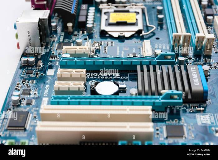
Comparison of Motherboard Size
| Component | Dimensions (approximate) |
|---|---|
| Standard ATX Motherboard | Around 305mm x 244mm |
| Playing Card | Around 88mm x 63mm |
The table above illustrates the significant difference in size between a standard motherboard and a playing card. The reduction in size achieved through miniaturization is substantial, allowing for the creation of compact and powerful devices.
Technological Processes
Shrinking a motherboard to playing card size represents a significant leap in miniaturization, demanding sophisticated technological processes. This involves not only reducing the size of components but also re-engineering the entire manufacturing pipeline. The complexity of these processes highlights the innovative spirit of engineers striving for compact, powerful electronic devices.
Methods of Miniaturization
Various methods are employed to shrink electronic components and circuits. Photolithography, a crucial technique, uses light to etch patterns onto materials, creating intricate circuit layouts. This method allows for precise control over the placement and size of components, enabling the fabrication of complex structures on a microscopic scale. Another method is etching, where chemicals selectively remove material to create desired shapes and patterns.
Advanced techniques like laser ablation and focused ion beam milling are also used to precisely sculpt components. These methods offer different levels of precision and control, with each having its advantages and limitations.
Materials Used in Miniaturized Motherboards
The materials selected for miniaturized motherboards are crucial for performance and reliability. High-density interconnects (HDIs) play a critical role in the reduced size by allowing multiple layers of interconnected circuits to be packed tightly together. The use of advanced polymers, such as epoxy resins, allows for improved thermal management and protection of sensitive components. The use of copper, gold, and other conductive materials is essential to maintain efficient signal transmission within the tight confines of the miniaturized board.
Careful material selection is vital to ensure that the miniaturized motherboard can withstand the stresses of operation and maintain its performance over time.
Manufacturing Techniques Comparison
Different manufacturing techniques have unique characteristics that affect the final product. Traditional printed circuit board (PCB) manufacturing methods, while reliable, might not be suitable for the ultra-small dimensions required for miniaturization. Advanced techniques like micro-fabrication processes offer greater control over component placement and size, enabling the creation of more complex and densely packed circuits. The choice of manufacturing technique often depends on the specific requirements of the miniaturized motherboard, including the complexity of the circuit, the desired yield, and the cost-effectiveness of the process.
For example, photolithography is widely used for its precision, while etching is favored for its ability to remove material selectively.
Challenges in Miniaturizing Electronic Components
Several challenges hinder the miniaturization of electronic components. One critical challenge is the thermal management of highly integrated circuits. As components shrink, heat dissipation becomes more challenging, potentially leading to overheating and performance degradation. The precise alignment and connection of components on a microscopic scale is another significant obstacle. Maintaining consistent quality and yield throughout the manufacturing process is also a significant concern, especially when dealing with complex and intricate designs.
Steps in the Manufacturing Process
The manufacturing process of a miniaturized motherboard is a complex multi-step procedure.
| Step | Description |
|---|---|
| 1 | Material Preparation: Selection and preparation of high-quality materials for the substrate, conductive traces, and dielectric layers. |
| 2 | Lithography: Precisely defining circuit patterns on the material using photolithography or other techniques. |
| 3 | Etching: Removing unwanted material to create the desired circuit patterns. |
| 4 | Metallization: Depositing conductive materials like copper or gold onto the etched patterns. |
| 5 | Assembly: Carefully assembling and connecting components onto the miniaturized motherboard. |
| 6 | Testing and Quality Control: Rigorous testing to ensure functionality, reliability, and performance standards. |
Impact on Electronic Devices
Shrinking motherboards to playing card size presents a fascinating opportunity to revolutionize electronic devices. This miniaturization process, while technically complex, unlocks potential for more compact, powerful, and energy-efficient gadgets. The implications for various industries, from consumer electronics to medical technology, are substantial. We’ll explore the specific benefits, performance considerations, and energy implications of this groundbreaking technology.Miniaturization affects the performance of electronic devices in several ways.
Crucially, the reduced size of components translates to lower overall device weight and volume. This is a significant advantage for portable devices. Furthermore, the closer proximity of components can potentially reduce signal transmission delays and enhance processing speed, though the impact is not always straightforward. The reduced size also has implications for heat dissipation, which needs careful consideration in design.
Potential Benefits for Different Devices
The advantages of miniaturizing motherboards are diverse and impact various electronic devices. Smaller form factors allow for enhanced portability, leading to more convenient use for a wide range of applications. Consider the implications for wearable technology, where size and weight are critical constraints. A miniaturized motherboard in a smartwatch, for instance, could enable more sophisticated functions without adding bulk.
- Enhanced Portability: Smaller form factors make devices more convenient and portable, ideal for wearables, handheld devices, and even embedded systems. The reduction in physical size significantly impacts usability, especially in applications requiring portability, like mobile phones and tablets. The lighter weight also contributes to a better user experience, making the devices easier to carry and use.
- Increased Computational Power (Potentially): While not always guaranteed, closer component placement in a miniaturized motherboard could theoretically lead to faster signal transmission and potentially higher processing speeds. This is contingent on careful design and engineering to mitigate potential issues.
- Improved Energy Efficiency: Miniaturization often leads to a reduction in power consumption, particularly in situations where heat dissipation is a challenge. The smaller size can contribute to a lower power consumption by minimizing the amount of energy required for operations and heat dissipation.
Performance Considerations
Miniaturization impacts the performance of electronic devices in complex ways. One crucial aspect is the potential reduction in signal transmission delays, which is often a consequence of shorter distances between components. However, challenges like heat dissipation and signal integrity must be addressed carefully. Modern designs prioritize these considerations, leading to increasingly compact and efficient systems.
- Signal Integrity: The proximity of components in a miniaturized design can affect signal integrity. Careful design is crucial to ensure signals remain clear and stable, preventing interference and errors.
- Heat Dissipation: Miniaturized designs can experience increased heat generation per unit area. Effective heat dissipation strategies are essential to prevent overheating and maintain optimal performance.
Energy Efficiency Comparison, Via shrinks motherboard to playing card size
A miniaturized motherboard, designed with careful attention to efficiency, can significantly improve energy efficiency compared to a standard motherboard. The smaller size can contribute to reduced power consumption by minimizing energy losses in components. However, the exact energy savings depend on the design and implementation.
Energy efficiency gains depend on meticulous design choices that minimize energy consumption during operation.
Miniaturized designs, when implemented well, can lead to substantial reductions in energy consumption, especially in mobile devices and other portable applications.
Examples of Benefiting Devices
Numerous devices could benefit from miniaturized motherboard technology. Wearable electronics, such as smartwatches and fitness trackers, would experience significant improvements in functionality and usability. Similarly, compact embedded systems, from medical implants to industrial sensors, could become even more powerful and integrated. The potential applications are wide-ranging.
- Smartwatches and Fitness Trackers: Miniaturization enables more sophisticated features and longer battery life, making these devices more functional and practical.
- Portable Medical Devices: Compact medical devices, including diagnostic tools and monitoring equipment, could benefit from smaller form factors, leading to improved portability and potentially lower costs.
- Industrial Sensors and Embedded Systems: Miniaturized motherboards facilitate more powerful and compact embedded systems for industrial applications, improving efficiency and performance.
Applications and Benefits Table
This table illustrates different applications and their corresponding benefits from miniaturized motherboard technology.
| Application | Benefits |
|---|---|
| Smartphones | Smaller size, potentially increased processing speed, improved energy efficiency |
| Wearable Devices | Enhanced functionality, improved battery life, smaller size |
| Medical Implants | Increased functionality, reduced size, potential for longer operation time |
| Industrial Sensors | Compactness, enhanced capabilities, improved integration |
Potential Applications and Markets
Miniaturized motherboards, shrunk to playing card size, unlock a wealth of possibilities across various industries. The unprecedented reduction in size, while maintaining functionality, opens doors to innovative designs and applications previously unimaginable. This technology promises to revolutionize consumer electronics, impacting everything from wearable devices to embedded systems.
Potential Markets
The potential markets for miniaturized motherboards are vast and diverse. These compact boards, capable of handling complex computing tasks, can be integrated into devices that were previously limited by size and power constraints. Their applicability spans beyond the realm of traditional consumer electronics, reaching into industrial automation and medical devices.
Product Examples
Numerous products can leverage the advantages of miniaturized motherboards. Imagine ultra-thin laptops that are as light as a tablet, yet with the processing power of a desktop. Wearable health monitors could become significantly more advanced, offering continuous, detailed data collection without compromising comfort. Smart home appliances, with their intricate control systems, can be integrated into smaller, more aesthetically pleasing designs.
Embedded systems for industrial applications, like robotic arms, can become more agile and responsive.
Applications by Industry
The potential applications are diverse and extend across various industries. The compact nature and increased processing power of these boards have a profound impact on several sectors.
- Consumer Electronics: Miniaturized motherboards allow for the creation of incredibly thin and lightweight devices like smartphones, tablets, and laptops, with superior processing power and battery life.
- Industrial Automation: These boards enable the development of more compact and efficient robotic systems and control mechanisms, improving response times and reducing overall system size.
- Medical Devices: Miniaturization allows for the creation of smaller, more portable medical diagnostic and monitoring tools, offering greater convenience for patients and healthcare professionals.
- Automotive: Integrating miniaturized motherboards into vehicles can lead to advanced driver-assistance systems, improved safety features, and potentially self-driving capabilities, while keeping the system compact.
- Aerospace: These boards can contribute to more compact and powerful avionics systems, improving efficiency and reducing weight, especially crucial for drones and smaller aircraft.
Market and Product Types
The table below illustrates a cross-section of potential markets and the corresponding types of products that could benefit from this technology.
| Potential Market | Corresponding Product Types |
|---|---|
| Consumer Electronics | Smartphones, Tablets, Ultra-thin Laptops, Wearable Devices |
| Industrial Automation | Compact Robots, Control Systems, Embedded Systems |
| Medical Devices | Portable Diagnostic Tools, Wearable Health Monitors |
| Automotive | Driver-Assistance Systems, Advanced Safety Features, Autonomous Vehicles |
| Aerospace | Avionics Systems, Drones, Small Aircraft |
Design Considerations and Challenges
Shrinking a motherboard to playing card size presents a fascinating engineering challenge, demanding innovative solutions to overcome numerous limitations. This miniaturization requires careful consideration of component placement, signal integrity, power delivery, and thermal management. The goal is not simply to reduce size, but to maintain or even enhance functionality and performance within the constrained space.The fundamental challenge lies in balancing the need for high performance with the severe limitations imposed by the extremely small footprint.
Miniaturization inevitably leads to trade-offs between size, cost, performance, and reliability. This section delves into the key design considerations and potential solutions for achieving a functional, playing-card-sized motherboard.
Component Placement and Interconnection
Careful planning and precise placement of components are crucial for a compact motherboard. The limited space necessitates a highly organized layout to ensure proper signal routing and minimize interference. High-density interconnects, such as advanced multilayer PCBs and through-hole technology, become critical to achieving the desired performance. This demands precise component selection and rigorous design verification to guarantee proper signal integrity.
Via’s incredible feat of shrinking motherboards to playing card size opens up exciting possibilities. This miniaturization, combined with a new protocol for maximizing wireless network communications, a new protocol for maximizing wireless network communications , promises to revolutionize portable tech. The implications for future devices are massive, potentially leading to even more compact and powerful systems that are far smaller than anything we currently have.
Signal Integrity and Noise
Miniaturization directly impacts signal integrity. Shorter signal paths, while beneficial in reducing latency, also increase the susceptibility to noise and crosstalk. Sophisticated signal integrity analysis and design techniques are required to mitigate these issues. Employing high-quality materials and specialized signal routing strategies are essential to maintaining reliable data transmission across the minimized circuitry.
Via’s recent advancements in shrinking motherboards to playing card size are truly impressive. This miniaturization, combined with innovative technologies like bt bridging mobile landline gap with dual mode devices , opens up exciting possibilities for portable electronics. The potential for even smaller, more powerful devices is incredibly exciting, and it’s a great leap forward for the future of tech.
Power Delivery and Efficiency
Efficient power delivery is paramount for a compact motherboard. Miniaturized power delivery systems, employing advanced power management ICs and ultra-low-profile components, must be designed to meet the increased power density. Optimizing power distribution networks and reducing power loss is critical for sustained performance and preventing overheating. Advanced power-saving techniques must be incorporated into the design to extend battery life.
Thermal Management and Heat Dissipation
Minimized space severely restricts heat dissipation options. Heat generated by components, especially in high-density designs, can quickly lead to overheating. Innovative cooling solutions, such as advanced heat sinks, embedded cooling modules, and passive cooling techniques, are crucial. Careful consideration of material selection and thermal conductivity of components is vital.
| Challenge | Potential Solution |
|---|---|
| Component Placement | Optimized layout algorithms, advanced placement software, 3D stacking of components |
| Signal Integrity | High-speed signal routing techniques, improved PCB materials, advanced signal integrity analysis tools |
| Power Delivery | Ultra-low-profile power components, advanced power management ICs, optimized power distribution networks |
| Thermal Management | Advanced heat sinks, embedded cooling modules, micro-channel cooling, novel heat dissipation materials |
Future Trends and Advancements: Via Shrinks Motherboard To Playing Card Size
The shrinking of electronics to playing card size opens a Pandora’s box of possibilities, hinting at a future where computing power and functionality are unprecedented. Miniaturization isn’t just about making things smaller; it’s about integrating more complex systems into incredibly compact spaces. This will drive innovation in various sectors, from medicine to transportation, and revolutionize how we interact with technology.
Potential Advancements in Miniaturization
Miniaturization techniques are constantly evolving, driven by the need for ever-smaller components. This involves exploring new materials, refining existing fabrication processes, and developing novel designs. One key area of advancement is in 3D printing technologies, enabling the creation of intricate, multi-layered structures. Another crucial factor is the development of advanced lithography techniques, allowing for even finer features and greater precision in the creation of microchips.
Ultimately, this pursuit of ever-smaller dimensions promises to push the boundaries of what’s possible in terms of device capabilities.
Future of Electronic Devices
Miniaturization will lead to a paradigm shift in electronic devices, paving the way for new and innovative gadgets. Imagine wearable devices that are not only powerful but also seamlessly integrated into our clothing or accessories. Imagine medical implants with unparalleled diagnostic capabilities, delivering real-time information and tailored treatments. Imagine incredibly compact computers with the processing power of today’s most advanced supercomputers, fitting into a palm-sized device.
Via’s shrinking of motherboards to playing card size is truly mind-blowing. Imagine the possibilities for smaller, more powerful devices, but with all this miniaturization, it’s crucial to consider security aspects. This kind of technology raises concerns about internet explorer’s security vulnerabilities, and users should seriously consider browser alternatives. internet explorer security concerns and browser alternatives Exploring more secure options will be paramount as these tiny motherboards become commonplace.
The future of computing is definitely looking compact and, hopefully, more secure!
The possibilities are limitless, with the potential for revolutionizing industries and personal lives.
Breakthroughs in Materials Science
Materials science plays a critical role in miniaturization. New materials must possess exceptional properties, such as high conductivity, flexibility, and biocompatibility. One promising area is the exploration of 2D materials like graphene and molybdenum disulfide, which exhibit extraordinary electrical and thermal properties. These materials could revolutionize the design of transistors, capacitors, and other crucial components. Also, the development of novel polymers with enhanced conductivity and flexibility opens doors for innovative packaging and flexible circuitry.
Table of Future Trends and Implications
| Future Trend | Potential Implications |
|---|---|
| Advancements in 3D printing for microelectronics | Creation of complex, multi-layered microchips and intricate device structures. |
| Development of novel 2D materials | Superior electronic properties, leading to faster and more energy-efficient transistors. |
| Integration of miniaturized sensors and actuators | Enhanced monitoring capabilities and advanced control systems in diverse fields like healthcare and robotics. |
| Increased computational power in smaller devices | Facilitates the development of portable, powerful tools for scientific research, data analysis, and everyday tasks. |
| Miniaturized medical implants | Real-time diagnostics and personalized treatment strategies for various medical conditions. |
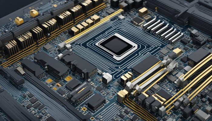
Illustration of Miniaturized Motherboard
Shrinking a motherboard down to the size of a playing card presents significant challenges, but also unlocks a wealth of possibilities. This level of miniaturization requires meticulous design and careful selection of components. The intricate layout and precise placement of each element are crucial for optimal performance and reliability. This section will explore the physical characteristics, component arrangement, and circuit diagrams of such a miniaturized motherboard.Miniaturized motherboards, while seemingly simple, are incredibly complex in their design and function.
The components, while significantly smaller, still need to perform the same functions as their larger counterparts. This requires a sophisticated understanding of materials science, circuit design, and fabrication techniques.
Physical Characteristics of a Miniaturized Motherboard
A miniaturized motherboard, designed for a playing card, will exhibit a compact form factor. Its physical dimensions will be constrained by the card’s size, dictating the overall size and shape of the board. The materials used for the board will likely be ultra-thin, high-density substrates, such as those made from ceramics or specialized polymers. Surface mount technology (SMT) will be almost exclusively used for component placement.
This will ensure maximum density while minimizing the overall board size.
Layout and Components of the Miniaturized Motherboard
The layout of the miniaturized motherboard is critical for efficient signal routing and heat dissipation. The arrangement of components, such as the CPU, memory chips, and input/output interfaces, must be optimized for minimal signal interference. High-density interconnects and careful routing are essential. The components themselves will be miniature versions of their larger counterparts, using advanced fabrication techniques to create incredibly small transistors and integrated circuits.
Illustration of the Motherboard on a Playing Card
Imagine a standard playing card. On one side, a very thin, almost transparent, circuit board is laid out, following the card’s Artikel. This board is the miniaturized motherboard. The circuit traces are incredibly fine, almost microscopic in width. Small, square components are positioned along the board.
These are the central processing unit (CPU), memory chips (RAM), and input/output (I/O) interfaces. The CPU, potentially a low-power microcontroller, sits centrally, connected to the other components by fine gold or copper traces. Memory chips, likely RAM or ROM, are positioned near the CPU, connected by similar traces. Small, specialized connectors or antenna-like structures are present for wireless communication.
Circuit Diagram of the Miniaturized Motherboard
The circuit diagram of the miniaturized motherboard reflects the precise connections between components. A simplified representation might show the CPU, memory, and I/O components as blocks connected by lines representing signal paths. The diagram will highlight the power supply and ground connections. Each component’s unique characteristics, such as input and output pins, are clearly depicted.
Function of Components
The miniaturized motherboard’s components are crucial for its function. Their detailed functions are listed below:
- Central Processing Unit (CPU): The CPU, a low-power microcontroller, is responsible for executing instructions and managing data flow. Its size is significantly reduced, using cutting-edge fabrication techniques.
- Random Access Memory (RAM): This temporary memory stores data currently being used by the CPU. Its size is reduced but retains the same functionality. Its reduced size necessitates advanced memory chip technology for optimal performance.
- Read-Only Memory (ROM): ROM stores the essential program code that boots up the device and contains the device’s initial instructions. Its reduced size and high density are essential for the miniaturized board.
- Input/Output (I/O) Interfaces: These interfaces connect the motherboard to external devices, such as sensors or actuators. Specialized, low-power interfaces are used for data exchange.
- Power Supply: This provides the necessary electrical power to the motherboard and its components. A tiny, high-efficiency power supply is necessary to provide the required power.
- Ground: The ground connection ensures proper electrical potential and stability throughout the circuit. It’s a critical component for proper function.
Epilogue
Via’s achievement in shrinking motherboards to playing card size marks a significant leap forward in electronics. This miniaturization, driven by ingenious technological advancements, opens up a world of possibilities for smaller, more powerful, and potentially more energy-efficient devices. The implications for consumer electronics, and beyond, are immense, and the future promises further innovation and exciting breakthroughs in this area.